
Silicon Wafer Scraps
A semiconductor plant requested a quote for the following.
We are looking for solar wafer scraps and silicon wafer scraps, if  you have any items in hand, Please provide.
- Quotation in US Dollars
- Thickness of the scraps
- Product Picture
- Packing
- Quantity
- Capacity per month
- The Soonest Delivery
Get Your Quote FAST! Or, Buy Online and Start Researching Today!
Scrap and broken silicon wafers, also known as silicon waste, have several potential applications and are often recycled or repurposed in various industries. Some common uses include:
- Solar cells: Broken or lower-grade silicon wafers can be used to manufacture solar cells, as the purity requirements for solar applications are less stringent than those for semiconductor devices.
- Electronics: Silicon waste can be used in the production of other electronic devices, such as sensors, microelectromechanical systems (MEMS), and radio frequency identification (RFID) tags.
- Metallurgical-grade silicon: Scrap silicon can be melted and purified to produce metallurgical-grade silicon, which is used in aluminum alloys, silicone products, and various chemical processes.
- Construction materials: Silicon waste can be incorporated into construction materials, such as concrete and asphalt, to improve their strength and durability.
- Abrasives: Crushed silicon waste can be used as an abrasive material for polishing, grinding, and sandblasting applications.
- Research and development: Scrap silicon wafers can be used in research and development projects, such as testing new processing techniques, equipment, or materials.
- Reclaim and reuse: In some cases, scrap silicon wafers can be reclaimed and reused in the semiconductor manufacturing process after undergoing proper cleaning and refurbishing procedures.
- Energy storage: Silicon waste can be used in the development of high-capacity anodes for lithium-ion batteries, improving their energy storage capabilities.
The recycling and repurposing of scrap and broken silicon wafers help reduce waste, conserve resources, and create value from materials that would otherwise be discarded.
Broken Silicon Wafer Applications in Research
Broken and scrap silicon wafers offer cost-effective materials for laboratory experiments, recycling, and semiconductor research. Depending on their condition and purity, these substrates may be repurposed for a variety of applications.
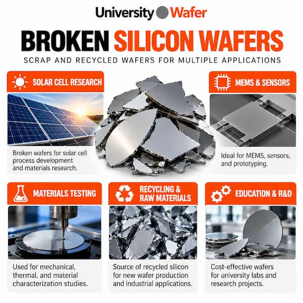
Common Research Applications
- Solar Cell Research: Suitable scrap silicon can be evaluated for photovoltaic research and material recovery.
- MEMS and Sensors: Selected wafer fragments may be used for MEMS research, process testing, and prototyping.
- Materials Testing: Silicon fragments can support mechanical, thermal, and semiconductor material characterization.
- Silicon Recycling: Scrap wafers can be processed for silicon recovery and potential industrial reuse.
- Education and R&D: Broken wafers provide inexpensive samples for university laboratories and experimental semiconductor processing.
Suitability depends on wafer purity, contamination, surface condition, and the requirements of each research application.
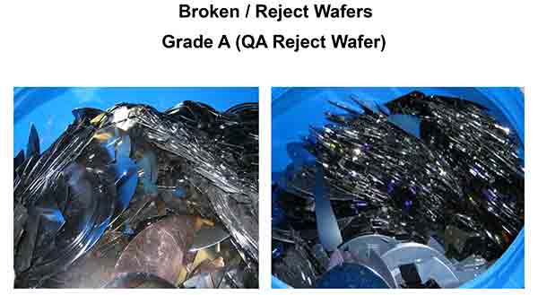
Broken and Rejected Silicon Wafer Inventory
Yes, we do have approx. 30-32 MT, now we keep them in our warehouses. Thickness of the broken wafers: 0.60-1.00mm (mostly 0.70-0.90 mm)
Packing: Packed in the drums
Q'ty: Aprrox. 30000-32000kgs in our own warehouse (Ready for Immediate delivery)
We have more available from other vendors, including different wafer diameters and substrate conditions.
Current Broken Silicon Wafer Inventory
| Pallet No. | Item | Size | Type | Amount (PCS) | Packing Type | Gross Weight (kg) | Net Weight (kg) | 가로 (mm) | 세로 (mm) | 높이 (mm) | Remarks |
|---|---|---|---|---|---|---|---|---|---|---|---|
| N/A | Film Mix / 700~730 um / P / High Res / No insert Paper | 300 mm | Notch / SEMI STD | 8 pcs/ Kg | 스티로폼 | N/A | 67,000 | 1100 | 1100 | 1250 | DUE TO List up |
| N/A | Film Mix / 720±25 um / P / High Res / No insert Paper | 200 mm | Flat / SEMI STD | 18 pcs/ Kg | 스티로폼 | N/A | 7,000 | 1100 | 1100 | 1250 | DUE TO List up |
| N/A | P / High Res / SEMI STD | Broken | N/A | N/A | 스티로폼 | N/A | 9,000 | 1100 | 1100 | 1250 | DUE TO List up |
| G-TOTAL | - | 83,000 |

200mm and 300mm Scrap Silicon Wafer Inventory
| Pallet No. | Item | Size | Type | Amount (PCS) | Packing Type | Gross Weight (kg) | Net Weight (kg) | 가로 (mm) | 세로 (mm) | 높이 (mm) | Remarks |
|---|---|---|---|---|---|---|---|---|---|---|---|
| 1 | Etched | 200mm | Flat & Notch | 13,158 | 스티로폼 | 761.0 | 731 | 1100 | 1100 | 900 | 2303 Update |
| 2 | Etched & SSP | 200&300 mm | Flat & Notch | 14,238 | 스티로폼 | 821.0 | 791 | 1100 | 1100 | 650 | 2303 Update |
| 3 | Etched & SSP | 200mm | Flat & Notch | 19,332 | 스티로폼 | 1104.0 | 1074 | 1100 | 1100 | 1138 | |
| 4 | Etched & SSP | 200mm | Flat & Notch | 16,686 | 스티로폼 | 957.0 | 927 | 1100 | 1100 | 1140 | |
| 5 | Film Mix | 200mm | Flat & Notch | 16,362 | PP BOX | 939.0 | 909 | 1100 | 1100 | 1090 | |
| 6 | Film Mix | 200mm | Flat & Notch | 14,310 | PP BOX | 825.0 | 795 | 1100 | 1100 | 1090 | |
| 7 | Bare + Film | 300 mm | Notch | 6,000 | 스티로폼 | 780.0 | 750 | 1100 | 1100 | 1250 | 2303 Updated |
| 8 | Bare | 300 mm | Notch | 6,600 | 스티로폼 | 855.0 | 825 | 1100 | 1100 | 1220 | |
| 9 | Film Mix | 300 mm | Notch | 7,705 | 스티로폼 | 1033.0 | 1003 | 1100 | 1100 | 1250 | |
| 10 | Film Mix | 300 mm | Notch | 7,755 | 스티로폼 | 1037.0 | 1007 | 1100 | 1100 | 1250 | |
| 11 | Film Mix | 300 mm | Notch | 7,765 | 스티로폼 | 1033.0 | 1003 | 1100 | 1100 | 1250 | |
| 12 | Film Mix | 300 mm | Notch | 7,760 | 스티로폼 | 1039.0 | 1009 | 1100 | 1100 | 1250 | |
| 13 | Film Mix | 300 mm | Notch | 7,615 | 스티로폼 | 1033.0 | 1003 | 1100 | 1100 | 1250 | |
| G-TOTAL | 145,286 | 11827 |
300mm Scrap Silicon Wafer Packaging

Related Silicon Wafer Research & Resources
Explore additional UniversityWafer resources about silicon wafer recycling, semiconductor materials, wafer processing, and research applications.
- Silicon Wafers for Research and Manufacturing
- Silicon Wafer Diameters and Sizes
- Silicon Wafer Thickness Specifications
- Silicon Wafer Dicing and Cutting
- Silicon Wafer Cleaning Methods
- Silicon Wafers for Solar Cell Research
- Silicon Substrates for MEMS and Sensors
- Silicon Wafer Resistivity Explained
- Test Grade Silicon Wafers for R&D