
Introduction to Semiconductor Materials
Semiconductor materials form the foundation of modern electronics, powering everything from consumer devices to advanced scientific equipment. These materials possess electrical 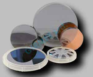 conductivity between insulators and conductors, making them uniquely valuable for controlling electrical current flow. The proper selection of semiconductor material is critical to the success of any electronic device or research project.
Choosing the right semiconductor involves balancing numerous factors including electrical properties, thermal characteristics, cost considerations, and application requirements. Whether you're developing power devices, electronic circuits, photoelectronics, or conducting academic research, your semiconductor material selection will significantly impact your results. Understanding semiconductor material properties is essential for making informed decisions.
As technology continues to evolve, understanding the fundamental properties and applications of different semiconductor materials becomes increasingly important. The semiconductor industry is constantly developing new materials and fabrication techniques to meet growing demands for smaller, faster, and more efficient devices.
Get Your Quote FAST! Or, Buy Online and Start Your Research Today!
Essential Factors When Selecting Semiconductor Materials:
- Consider the bandgap energy for your specific application requirements
- Evaluate carrier mobility and concentration for optimal device performance
- Assess thermal conductivity for heat management in your devices
- Choose between silicon, compound semiconductors, or specialized materials based on performance needs
- Factor in manufacturing complexity and cost considerations
- Consider environmental conditions where the semiconductor will operate
Understanding Basic Semiconductor Properties
When selecting semiconductor materials, it's essential to understand several fundamental properties that determine their performance in various applications. These properties dictate how the material will behave under different conditions and whether it's suitable for your specific needs.
Bandgap Energy and Its Significance
The bandgap energy of a semiconductor is perhaps its most defining characteristic. This property represents the energy difference between the valence band and the conduction band, determining how easily electrons can move from one band to another. Materials with smaller bandgaps (like silicon at 1.1 eV) are easier to excite thermally, while those with larger bandgaps (like gallium phosphide at 2.24 eV) require more energy for electron excitation.
The bandgap determines the operating temperature range, light emission wavelength (for LEDs and lasers), switching speed in electronic devices, and overall suitability for specific applications like solar cells or power electronics.
Carrier Mobility and Concentration
Carrier mobility refers to how quickly electrons and holes can move through the semiconductor material when an electric field is applied. Higher mobility generally results in faster device operation. Carrier concentration indicates the number of free carriers available for conduction.
Different semiconductor materials exhibit vastly different carrier mobilities. Silicon offers moderate mobility suitable for many general applications. Gallium arsenide provides higher mobility than silicon, making it preferred for high-frequency applications. Lithium niobate is used in specialized applications requiring unique electro-optical properties.
Thermal Conductivity and Stability
Thermal properties are crucial for device reliability and performance. Semiconductors with high thermal conductivity can dissipate heat more efficiently, allowing for higher power operation without degradation. When selecting materials for high-power applications, thermal conductivity becomes a critical factor. Materials like silicon carbide offer superior thermal conductivity compared to standard silicon, making them ideal for power electronics that generate significant heat during operation.
Silicon on insulator (SOI) wafers provide excellent thermal isolation properties, making them particularly valuable for applications where thermal management is critical. The insulating layer in SOI wafers helps prevent heat transfer to the substrate, enabling more efficient device operation.
Silicon: The Standard Bearer of Semiconductor Materials
Silicon remains the most widely used semiconductor material in the industry, serving as the foundation for most electronic devices. Its abundance, well-established processing techniques, and balanced properties make it the default choice for many applications.
Advantages of Silicon-Based Semiconductors
Silicon offers numerous advantages that have cemented its position as the dominant semiconductor material. First, it's the second most abundant element in the Earth's crust, making it relatively inexpensive compared to other semiconductor materials. Second, decades of development have resulted in highly refined silicon processing techniques, allowing for mass production with excellent quality control. Third, silicon naturally forms silicon dioxide (SiO₂) when oxidized, which serves as an excellent insulator in integrated circuits. Finally, with a bandgap of 1.1 eV, silicon is well-suited for room temperature operation in many applications.
Silicon Variants and Specialized Forms
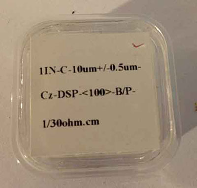
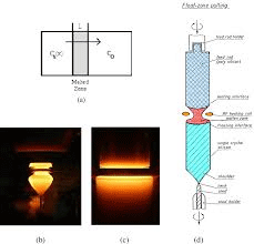
While standard silicon is widely used, several specialized forms offer enhanced properties for specific applications. Float Zone (FZ) silicon is a highly specialized method of growing silicon crystals that results in extremely pure material with minimal oxygen content. This makes it ideal for high-performance applications where impurities would degrade device performance. Key benefits include ultra-high purity with minimal defects, excellent performance for power devices and high-frequency applications, and superior performance in photoelectronic applications.
Silicon on Insulator (SOI) wafers consist of a thin layer of silicon on top of an insulating material, typically silicon dioxide. This structure offers significant advantages for certain applications, including low power applications, fast devices requiring excellent isolation from the substrate, MEMS and CMOS applications where substrate isolation is critical, and radiation-hardened electronics for space applications.
Ultra-thin silicon wafers offer advantages for specific applications where standard thickness wafers would be unsuitable. These wafers are typically thinned down to tens of microns, compared to standard wafers that are hundreds of microns thick. Benefits include improved light absorption for solar applications, reduced material usage and weight, enhanced flexibility for certain applications, and better heat dissipation in some configurations.
Compound Semiconductors: Beyond Silicon
While silicon dominates the semiconductor industry, compound semiconductors—materials composed of two or more elements—offer properties that silicon cannot match. These materials are increasingly important for specialized applications that require superior performance in specific areas.
III-V Semiconductors
III-V semiconductors are composed of elements from groups III and V of the periodic table. These materials often exhibit superior electron mobility and direct bandgaps, making them ideal for optoelectronic applications. III-V materials are crucial for high-performance devices, and factors like bandgap, thermal conductivity, and electron mobility are important considerations when choosing these materials.
Gallium Phosphide (GaP) is a compound semiconductor with an indirect bandgap of 2.24 eV. This material offers several advantages for specific applications including high conductivity with excellent oxidation resistance, extensive use in the fabrication of LEDs (particularly green LEDs), suitability for high-temperature and high-power applications, and excellent optical properties for certain wavelengths.
Other Specialized Semiconductor Materials
Beyond the common III-V semiconductors, several other specialized materials offer unique properties for specific applications. Lithium Niobate (LiNbO₃) is a versatile material with exceptional electro-optical, piezoelectric, and nonlinear optical properties. While not a traditional semiconductor, it's widely used in optoelectronic applications.
Key applications for LiNbO₃ include surface acoustic wave (SAW) devices, optical modulators and switches, frequency doublers and parametric oscillators, and integrated optical circuits. Our inventory includes various grades and cuts of LiNbO₃ wafers, including SAW grade, optical grade substrates, and stoichiometric LiNbO₃ (SLN) wafers for specialized requirements.
Sapphire (Al₂O₃) is not a semiconductor itself but serves as an excellent substrate for growing various semiconductor materials, particularly gallium nitride (GaN) for LED applications. Sapphire is a preferred substrate material for many applications with excellent thermal conductivity and chemical inertness. It offers several advantages as a substrate material including extreme durability and chemical inertness, excellent thermal stability, transparency to a wide range of wavelengths, and lattice matching capabilities for certain semiconductor materials.
Application-Specific Material Selection Criteria
Choosing the right semiconductor material requires careful consideration of the specific application requirements. Different applications prioritize different material properties, making the selection process highly context-dependent.
Electronics and Computing Applications
For electronic devices and computing applications, key considerations include switching speed, power consumption, integration density, and reliability. Materials with higher carrier mobility enable faster switching, which is critical for high-performance computing. Low-power applications often benefit from materials like SOI that reduce leakage current.
The ability to create smaller features enables higher transistor counts and more complex circuits. Materials must also maintain stable performance over time and under various operating conditions. Our semiconductor materials catalog includes options optimized for various electronic applications, from general-purpose computing to specialized high-performance devices.
Optoelectronic and Photonic Applications
Optoelectronic devices like LEDs, lasers, and photodetectors require materials with specific optical properties. Direct bandgap materials (like most III-V semiconductors) are more efficient for light emission and absorption. The bandgap energy determines the wavelength of emitted or absorbed light, which is critical for applications like LEDs and solar cells.
For optical waveguides and windows, materials must be transparent to the wavelengths of interest. Materials like lithium niobate offer excellent electro-optic properties for modulators and switches.
Key Considerations for Semiconductor Selection by Application Type
- Computing & Electronics - Prioritize carrier mobility, integration density, and power efficiency
- Optoelectronics - Consider bandgap type (direct vs. indirect), absorption/emission wavelengths, optical transparency, and electro-optic properties
- Power Electronics - Focus on breakdown voltage, thermal conductivity, and minimizing switching losses
- Solar Applications - Evaluate absorption coefficient, bandgap matching to solar spectrum, and energy harvesting efficiency
- High Temperature Applications - Select wide bandgap semiconductors (SiC, GaN) that can operate at temperatures up to 300°C compared to silicon's 150°C limit
- High Frequency Applications - GaN offers higher electron mobility (2000 cm²/Vs) compared to silicon (1500 cm²/Vs) and SiC (650 cm²/Vs)
- Radiation-Resistant Applications - Consider wide-bandgap materials like GaN, ZnO, and β-Ga₂O₃ which demonstrate superior radiation tolerance
- High Power Density Applications - SiC has superior thermal conductivity (5 W/cmK) compared to GaN (1.3 W/cmK) and silicon (1.5 W/cmK)
- High Voltage Applications - SiC and GaN offer approximately 10x higher breakdown field strength compared to silicon
- Cost-Sensitive Applications - Silicon remains most cost-effective, comprising 85% of semiconductor materials with abundant supply
Source: UniversityWafer, Inc.
Energy Harvesting and Solar Applications
For solar cells and other energy harvesting applications, semiconductor material selection focuses on absorption coefficient, bandgap matching, carrier lifetime, and cost and scalability. The absorption coefficient determines how efficiently the material absorbs photons of specific wavelengths. Optimal bandgaps for single-junction solar cells are typically around 1.4-1.5 eV to match the solar spectrum.
Longer carrier lifetimes reduce recombination losses, improving solar cell efficiency. Practical solar applications require cost-effective materials that can be manufactured at scale. Our solar cell materials include various options for research and development, including dye-sensitized solar cell components and ultra-thin silicon wafers optimized for improved light absorption.
Manufacturing and Processing Considerations
The selection of semiconductor materials is heavily influenced by manufacturing and processing requirements. Even materials with ideal electrical properties may be impractical if they cannot be reliably manufactured or integrated into existing processes.
Material Purity and Defect Density
Semiconductor performance is highly sensitive to impurities and crystallographic defects. Different applications have varying tolerance levels for these imperfections. High-performance electronics require extremely pure materials with minimal defects to ensure reliable operation and high yields. Power devices can often tolerate higher defect densities in exchange for other beneficial properties like wider bandgaps. Research applications may require ultra-pure materials for fundamental studies or proof-of-concept devices.
Float Zone silicon offers exceptional purity with minimal oxygen content, making it ideal for applications where impurities would significantly degrade device performance. It's a high-purity silicon material used for semiconductor applications with purity levels exceeding 99.9999%.
Cost and Availability Factors
Practical semiconductor material selection must consider economic factors alongside technical requirements. The cost and availability of materials can significantly impact project feasibility and commercial viability. Semiconductor materials vary widely in cost, influenced by factors such as raw material abundance, processing complexity, wafer size, and volume requirements.
For research projects with limited budgets, consider using reclaimed or test-grade wafers that may have cosmetic imperfections but still offer acceptable electrical properties. University Wafer offers various grade options to accommodate different budget constraints while maintaining the necessary quality for successful research outcomes.
The reliability and stability of the supply chain are also critical factors, especially for production environments. Depending on a single source for critical materials can introduce significant risk. Some semiconductor materials involve elements subject to supply restrictions or geopolitical tensions. Specialized materials often have longer lead times, which must be factored into project planning. The availability of custom specifications (thickness, doping, orientation) varies by material and supplier.
Conclusion: Making the Right Semiconductor Material Choice
Selecting the optimal semiconductor material requires balancing various technical, economic, and practical considerations. Begin by clearly defining your application requirements, including performance metrics, operating conditions, size constraints, and reliability needs. Then prioritize material properties based on your specific application, identifying critical "must-have" properties and acceptable trade-offs.
Consider practical implementation aspects such as manufacturing capability, integration challenges, testing requirements, and regulatory compliance. Different applications demand different semiconductor materials - silicon remains the workhorse for many general applications, while specialized materials like III-V compounds, SOI, and wide-bandgap semiconductors offer superior performance for specific use cases.
At University Wafer, we offer a comprehensive range of semiconductor materials to meet diverse research and production needs. Our experts can help you navigate the selection process, ensuring you choose the right material for your specific application. Whether you need standard silicon wafers, specialized float zone silicon, gallium phosphide, or other advanced materials, we provide high-quality products tailored to your requirements.
Remember that the best semiconductor material choice depends on your specific application requirements, budget constraints, and performance goals. By carefully considering the factors outlined in this guide, you can make an informed decision that optimizes your device performance while meeting practical manufacturing and economic considerations.