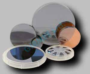
What is Gallium Phosphide?
Gallium phosphide is a compound semiconductor with an indirect band gap of 2.24 eV at room temperature. It is a pale orange to grayish material with pieces of a crystal structure. It is a semiconductor with a high intrinsic mobility (a high resonant frequency) and is a good candidate for use in batteries and solar cells. For this reason, the compound is highly conductive and exhibits excellent oxidation resistance.
Get Your Quote FAST! Or, Buy Online and Start Researching Today!
Other Wafers Include
- Aluminum (Al) Wafers
- Germanium (electrical and optical Grades)
- Graphene
- LiNbO3
- Lithium Tantalate (LiTaO₃) Wafers
- Silicon on Insulator
- Silicon on Sapphire
- GaN/AlN on Sapphire
- InGaAs
Related Materials and Semiconductor Resources
Gallium Phosphide (GaP) Wafers
In semiconductors, gallium phosphide is a type III-V compound semiconductor that has a wide indirect band  gap. The crystal structure of this compound is the same as silicon. Its lattice constant is 0.545 nm and its electron and hole mobility are approximately 100 and 75 cm2/V-s, respectively. This material is insoluble in water and odorless. It has been used in the fabrication of many electronic devices, including CMOS and RF/V/A switches.
The main substrate material for LEDs is gallium phosphide, and it is transparent to red, yellow and orange light. This characteristic makes gallium phosphide a superior choice for LEDs. These diodes are transparent to most light, so their use in electronic components depends on how brightly they emit light. However, there is a problem associated with this material. Although it is highly conductive, it does not emit enough light to be useful as a source of illumination.
The energy gap of gallium phosphide is 2.24 eV, making it an ideal material for use in electronics.
The main disadvantages of gallium phosphide are its high cost and low sensitivity. It also tends to lose its brightness at high temperatures and is prone to thermal instability. Despite its low price and low sensitivity, it has many other advantages. For example, it can be used in inexpensive LEDs. Its optical properties are excellent, but it does not have a wide temperature range. Further, it is odorless and transparent, which makes it suitable for applications ranging from medical equipment to household appliances.
As a nonlinear semiconductor, gallium phosphide has an indirect bandgap and is transparent to visible and long-infrared wavelengths. However, its use in nanophotonic devices has been limited, largely due to the fact that it has little been studied as an integrated photonic material. For instance, a single-crystalline gallium phosphide is highly efficient, but it lacks high-resolution transparency.
Order GaP Wafers and Other Substrates Online!
Gallium Phosphide (GaP) Wafer Inventory
Below are just some of the available GaP substrates.
GaP Wafer undoped (100) 2"x 0.5 DSP
GaP Wafer, Undoped (111) 10x10x0.35 mm, DSP
GaP Wafer, Undoped (111) 10x10x0.5 mm, DSP
GaP Wafer, S doped (111) 2"x0.5 mm, DSP
GaP Wafer, undoped (100) 10x10x0.5 mm, SSP
GaP Wafer, undoped (100) 10x10x0.5 mm, DSP
GaP Wafer, undoped (100) 10x3x0.5 mm, SSP
GaP wafer undoped (100) 2" diaX 0.45mm SSP, R: 1.5x10^14 ohm.cm, Semi-Insulating
GaP wafer, S doped, (100), 2" dia x 0.5 mm, SSP
GaP wafer, S doped, (100), 2" dia x 0.50 mm, DSP
GaP wafer, S doped, (100), 5 x 5 x 0.5 mm, SSP
GaP Wafer, undoped (110) 10x10x0.45 mm, SSP
GaP Wafer, undoped (110) 10x10x0.5 mm, DSP
GaP Wafer, undoped (110) 5x5x0.2 mm, DSP
