
Epi Silicon Vs Standard Silicon Substrates
Key Takeaways
- Epitaxial silicon wafers have an additional crystalline layer grown on a substrate, while standard wafers are uniform single-crystal structures
- Epitaxial wafers offer better electrical performance, more precise doping control, and fewer defects than standard wafers
- Standard silicon wafers cost less and work well for applications that don't need the special properties of epitaxial layers
- Epitaxial wafers are crucial for advanced semiconductor devices like power electronics and high-performance integrated circuits
- The manufacturing processes for the two wafer types differ significantly, with epitaxial growth requiring specialized equipment
Get Your Quote FAST! Or, Buy Online and Start Your Research Today!
Introduction to Silicon Wafer Types
Silicon wafers form the foundation of modern electronics, serving as the primary material for semiconductor devices and integrated circuits. When selecting silicon wafers for specific applications, understanding the differences between epitaxial and standard silicon wafers is crucial.
Standard silicon wafers are uniform, single-crystal structures sliced from a silicon ingot. These wafers serve as the basic building blocks for many semiconductor applications. Silicon ingots are carefully grown using methods like the Czochralski process to ensure high purity before being sliced into wafers.
Epitaxial silicon wafers, on the other hand, feature an additional crystalline layer grown on top of a silicon substrate. This epitaxial layer can be precisely controlled in terms of thickness and doping concentration, offering enhanced electrical properties compared to standard wafers.
The choice between epitaxial and standard silicon wafers depends on your specific application requirements. In this guide, we'll explore the main differences, manufacturing processes, properties, applications, and cost considerations to help you make an informed decision for your research or production needs.
Fundamentals of Epitaxial Silicon Wafers
What is Epitaxy?
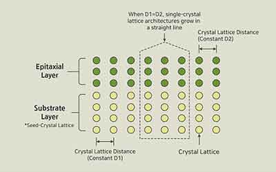
Epitaxy comes from the Greek words "epi" (above) and "taxis" (in an ordered manner), referring to the process of growing a crystalline layer on a crystalline substrate. In semiconductor manufacturing, epitaxy involves depositing a thin layer of single-crystal material onto a single-crystal substrate, where the deposited layer follows the crystal orientation of the underlying substrate.
Epitaxial growth can be classified into two main types:
- Homoepitaxy: When the epitaxial layer and the substrate are the same material (e.g., silicon on silicon). This is the most common type used in epitaxial silicon wafers for semiconductor applications.
- Heteroepitaxy: When the epitaxial layer and substrate are different materials (e.g., gallium arsenide on silicon). This type is used for specialized applications like optoelectronics.
The epitaxial layer's thickness can range from a few atomic layers to several microns, depending on the intended application. For most semiconductor devices, epitaxial layers typically range from 2μm to 150μm.
Manufacturing Process of Epitaxial Wafers
The production of epitaxial silicon wafers involves several sophisticated techniques, with Chemical Vapor Deposition (CVD) being the most common method used in industrial settings. The process typically follows these steps:
- First, a standard silicon wafer serves as the substrate and undergoes thorough cleaning to remove any contaminants.
- Then, the substrate is placed in a reaction chamber where it's heated to temperatures between 900°C and 1250°C.
- Precursor gases like silane (SiH₄) or silicon tetrachloride (SiCl₄) are introduced into the chamber.
- During layer growth, the precursor gases break down at the hot substrate surface, depositing silicon atoms that arrange themselves according to the crystal structure of the substrate.
- For doping, gases like diborane (B₂H₆) for p-type doping or phosphine (PH₃) for n-type doping can be added to achieve the desired electrical properties.
- After the epitaxial layer reaches the desired thickness, the wafer is cooled and inspected for defects, thickness uniformity, and resistivity.
At University Wafer, we maintain strict quality control throughout the manufacturing process to ensure our epitaxial wafers meet the highest standards.
Standard Silicon Wafer Fundamentals
Structure and Properties
Standard silicon wafers are single-crystal substrates sliced from a silicon ingot. These wafers serve as the foundation for most semiconductor devices and integrated circuits. The properties of standard silicon wafers are determined by the crystal growth method, doping type and concentration, and the subsequent processing steps.
Key characteristics of standard silicon wafers include:
- Crystal Orientation: Typically available in (100), (111), or (110) orientations, with (100) being the most common for CMOS applications.
- Doping Type: Available as p-type (typically boron-doped) or n-type (typically phosphorus or arsenic-doped).
- Resistivity Range: From less than 0.001 ohm-cm for heavily doped wafers to over 10,000 ohm-cm for high-resistivity applications.
- Thickness: Standard thicknesses vary by diameter, typically ranging from 275μm to 775μm.
- Surface Finish: Available with various surface finishes including prime grade (polished), test grade, and mechanical grade.
Manufacturing Process of Standard Wafers
The production of standard silicon wafers involves several steps:
- It starts with silicon purification, where metallurgical-grade silicon (98% pure) is converted to electronic-grade silicon (99.9999999% pure) through chemical processes.
- Then, single-crystal silicon ingots are grown using methods like the Czochralski (CZ) process or Float Zone (FZ) technique.
- Next, the ingot undergoes grinding to achieve the desired diameter and to mark the crystal orientation.
- The ingot is then sliced into thin wafers using diamond wire saws, with each slice typically 500-700μm thick.
- The wafer edges are rounded to reduce the risk of chipping and to improve handling safety.
- The wafers then undergo lapping to improve flatness, followed by etching to remove surface damage.
- For prime-grade wafers, chemical-mechanical polishing (CMP) is performed to achieve a mirror-like surface finish.
- Finally, the wafers undergo rigorous cleaning and inspection to ensure they meet the required specifications.
Key Differences Between Epitaxial and Standard Silicon Wafers
Structural Differences
The fundamental structural difference between epitaxial and standard silicon wafers lies in their composition:
Standard silicon wafers consist of a single, uniform crystal structure throughout the entire wafer. They have relatively consistent doping concentration throughout the bulk and may contain crystal defects and impurities distributed throughout the wafer.
Epitaxial silicon wafers feature a distinct, high-quality epitaxial layer grown on top of a substrate. They often have different doping types or concentrations between the substrate and epitaxial layer and can have a buried layer or multiple epitaxial layers for specialized applications.
This structural difference creates a clear boundary between the epitaxial layer and the substrate in epitaxial wafers, which can be advantageous for certain device designs. The epitaxial layer typically has fewer defects and more precisely controlled properties compared to the bulk substrate.
Electrical Property Differences
The electrical properties of epitaxial and standard silicon wafers differ significantly:
For doping control, standard wafers have doping introduced during crystal growth, resulting in relatively uniform but less precisely controlled doping concentrations. Epitaxial wafers can have doping precisely controlled during the epitaxial growth process, allowing for complex doping profiles and abrupt junctions.
Regarding resistivity, standard wafers typically have uniform resistivity throughout the wafer, with values ranging from <0.001 ohm-cm to >10,000 ohm-cm. Epitaxial wafers can have different resistivity values in the substrate and epitaxial layer, with the epitaxial layer tailored to specific resistivity requirements.
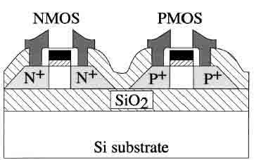
For latch-up prevention, standard wafers are more susceptible to latch-up phenomena in CMOS circuits, while the epitaxial structure with highly doped substrate reduces parasitic effects and prevents latch-up, making them ideal for high-performance CMOS applications.
Defect Density and Quality
The quality and defect characteristics also differ between the two wafer types:
For crystal defects, standard wafers may contain various crystal defects from the crystal growth process, including oxygen precipitates, dislocations, and slip lines. Epitaxial wafers typically have significantly fewer defects in the epitaxial layer than the substrate, as it's grown under carefully controlled conditions.
Regarding impurity gettering, standard wafers often require additional processing steps for gettering (the process of removing impurities). In epitaxial wafers, the interface between the substrate and epitaxial layer can act as a natural gettering site, trapping impurities away from the active device region.
For surface quality, standard wafers' surface quality depends primarily on the polishing process. Epitaxial wafers provide a fresh, high-quality surface with excellent flatness and fewer surface defects.
Applications and Use Cases
Ideal Applications for Epitaxial Wafers
Epitaxial silicon wafers excel in applications that require precise control of electrical properties and high performance:
For power devices, they're used in high-voltage power MOSFETs, Insulated Gate Bipolar Transistors (IGBTs), power diodes, and Silicon Controlled Rectifiers (SCRs). In bipolar integrated circuits, they're used for high-speed bipolar logic, analog circuits, RF amplifiers, and operational amplifiers.
For advanced CMOS processes, epitaxial wafers are used in latch-up resistant CMOS circuits, deep sub-micron CMOS devices, and low-noise analog CMOS circuits. They're also used in radiation-hardened devices for space and military electronics, nuclear instrumentation, and medical imaging equipment.
Silicon carbide wafers with epitaxial layers are particularly valuable for high-temperature, high-power applications like electric vehicle power systems and renewable energy converters.
Ideal Applications for Standard Wafers
Standard silicon wafers are well-suited for a broad range of applications where the enhanced properties of epitaxial layers aren't critical:
They're used in general-purpose integrated circuits like memory chips (DRAM, Flash), microcontrollers, standard logic devices, and consumer electronics. They're also used in MEMS and sensors such as pressure sensors, accelerometers, gyroscopes, and microfluidic devices.
Standard wafers are also used in photovoltaic cells, including solar cells, photodetectors, and optical sensors. They're commonly used in research and development for process development, materials research, educational purposes, and prototype fabrication.
Standard silicon wafers are also commonly used as starting materials for creating more specialized substrates like Silicon-on-Insulator (SOI) wafers through additional processing steps.
Cost and Economic Considerations
Manufacturing Cost Comparison
The manufacturing processes for epitaxial and standard silicon wafers differ significantly in complexity and resource requirements, leading to notable cost differences:
Standard silicon wafers have lower production costs due to simpler manufacturing processes. They benefit from economies of scale in high-volume production, and processing costs increase with larger diameters but at a lower rate than epitaxial wafers. They typically cost between $5-$300 per wafer depending on diameter, quality grade, and specifications.
Epitaxial silicon wafers have higher production costs due to the additional epitaxial growth process. They require specialized equipment and controlled environments, and gas precursors and dopants add to material costs. The process complexity increases with epitaxial layer thickness and doping requirements. They typically cost between $20-$1000+ per wafer depending on specifications.
Selection Guide: Choosing Between Epitaxial and Standard Wafers
Selecting the right wafer type requires careful consideration of multiple factors:
First, assess your application requirements. Identify whether you're building power devices, integrated circuits, MEMS, or other devices. Determine the critical electrical parameters for your application and consider voltage, current, frequency, and temperature requirements.
Next, match technical specifications. Decide if you need the distinct layers provided by epitaxial wafers, assess whether your device requires precise doping control, and determine how sensitive your devices are to crystal defects.
Finally, consider economic factors. Consider your available funding for wafer procurement, determine whether you need small quantities for research or larger volumes for production, and assess whether the performance benefits of epitaxial wafers justify their cost.
Conclusion
Choosing between epitaxial and standard silicon wafers involves careful consideration of technical requirements, application needs, and economic factors. Both wafer types have their place in semiconductor manufacturing and research, with distinct advantages for different use cases.
Epitaxial wafers feature a high-quality crystalline layer grown on a substrate, while standard wafers have a uniform structure throughout. The epitaxial layer can be precisely controlled in terms of thickness and doping concentration, offering superior electrical performance, better defect control, and enhanced latch-up immunity compared to standard wafers.
Power devices, high-performance integrated circuits, and radiation-hardened applications benefit significantly from epitaxial wafers. Meanwhile, general-purpose ICs, MEMS devices, and research applications can often use standard wafers effectively.
While epitaxial wafers have higher manufacturing costs, they may provide better overall value through improved device performance and yields. Standard wafers offer cost advantages for applications where the enhanced properties of epitaxial layers aren't critical.
For researchers, engineers, and manufacturers trying to decide between epitaxial and standard silicon wafers, we recommend:
- Start with your application requirements and clearly define the technical needs of your devices or experiments
- Consider the full value chain beyond initial wafer costs
- Seek expert guidance from our technical team at University Wafer for personalized recommendations
- Begin with small quantities for new projects to validate your requirements before scaling up
At University Wafer, we're committed to helping you navigate these choices with expert guidance, competitive pricing, and a wide range of both standard and epitaxial silicon wafers to meet your specific needs. Whether you're conducting cutting-edge research or developing commercial products, we provide the high-quality semiconductor materials that form the foundation of your success.
Contact us today to discuss your silicon wafer requirements and let our experienced team help you select the optimal wafer type for your application.