
Essential Points About Lithography for Silicon Wafers
- Lithography is a fundamental process in semiconductor manufacturing that creates intricate patterns on silicon wafers
- Multiple lithography techniques exist, including photolithography, e-beam lithography, and soft lithography
- The choice of lithography method depends on application requirements, resolution needs, and production volume
- Silicon substrates serve as the primary foundation for most lithography processes in semiconductor manufacturing
- Advanced etching techniques work in conjunction with lithography to create three-dimensional structures
- Continued advancement in lithography technology enables the ongoing miniaturization of electronic components
Get Your Quote FAST! Buy Online and Start Researching Today!
Introduction to Silicon Wafer Lithography
Lithography is like drawing incredibly tiny pictures on silicon wafers. These pictures become the patterns for all the electronic parts in our phones, computers, and other gadgets. Think of it as using a super-precise pencil to draw lines thousands of times thinner than a human hair! Without lithography, we wouldn't have any of the electronic devices we use every day. This fundamental process serves as the cornerstone of modern semiconductor manufacturing, enabling the creation of increasingly complex integrated circuits and microelectronic devices that power our digital world.
The coolest thing about lithography is how it keeps letting engineers make smaller and smaller electronic parts. Back in the 1970s, the smallest features on computer chips were about as wide as a red blood cell. Today, thanks to advanced lithography, we can make features that are thousands of times smaller! This is why your phone today is way more powerful than the biggest computers from decades ago, even though it fits in your pocket.
Silicon wafers are perfect for lithography because they're super flat, pure, and have special electrical properties. At University Wafer, researchers and companies can get silicon wafers that are specially made for different types of lithography. These wafers need to be incredibly clean and smooth - even a tiny speck of dust could ruin the patterns!

Silicon Wafers: The Foundation of Lithography Processes
Before we dive into the cool ways scientists draw tiny patterns, let's talk about the special discs they draw on. Silicon wafers are thin, round slices of super-pure silicon crystal. Think of them like blank canvases that will eventually become the brains of our computers, phones, and other electronic gadgets.
These wafers have to be incredibly flat - flatter than a sheet of paper if you scaled it up. Even tiny bumps or dips that are smaller than a virus could mess up the patterns. The silicon also needs to be extremely pure, with less than one impurity for every billion silicon atoms! Scientists control exactly how electricity flows through the wafer by adding tiny amounts of other elements like phosphorus or boron.
Different types of electronic devices need different kinds of silicon wafers. Some need wafers with a specific crystal direction (like <100> or <111>), which affects how the silicon atoms are arranged. Others need wafers with particular electrical properties or special coatings. At University Wafer, researchers can get exactly the right type of silicon wafer for their specific lithography needs.
Safety Considerations for Silicon Wafer Handling
Working with silicon wafers isn't as simple as handling regular materials. Silicon dust can be harmful if you breathe it in, and the edges of wafers can be surprisingly sharp - they can cut you like paper cuts but worse! Scientists and engineers always wear special gloves, face masks, and sometimes even full clean room suits when handling these materials.
Clean rooms where silicon wafers are processed are super clean environments - much cleaner than a hospital operating room. The air is constantly filtered to remove dust particles that could ruin the tiny patterns. Workers wear special clothing that doesn't shed fibers and follow strict procedures to prevent contamination.
If you're working with silicon wafers, it's important to know how to handle them safely. University Wafer provides detailed safety information for all their silicon products, explaining how to properly handle the wafers and what to do in case of an emergency.
Photolithography: The Workhorse of Semiconductor Manufacturing
Photolithography is the most common way to make patterns on silicon wafers. It's like using a super-advanced version of the process used to make T-shirts! Imagine shining light through a stencil to create a pattern, but instead of fabric paint, you're using special chemicals that change when exposed to light, and instead of a T-shirt, you're patterning a silicon wafer that will become thousands of computer chips.
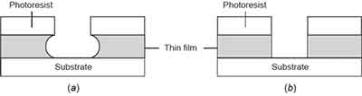
The process starts by coating the silicon wafer with a light-sensitive chemical called photoresist. Then, a mask (like a stencil) containing the desired pattern is placed above the wafer. When ultraviolet light shines through the mask, it changes the photoresist in the exposed areas. Depending on the type of photoresist, either the exposed or unexposed areas can be washed away with a special solution, leaving behind the pattern. This pattern then guides further steps like etching or adding materials to build up the layers of a computer chip.
Photolithography has improved dramatically over the years. Early systems used visible light, but modern systems use deep ultraviolet light with wavelengths as short as 193 nanometers. Some cutting-edge systems even use extreme ultraviolet light with wavelengths of just 13.5 nanometers! The shorter the wavelength, the smaller the features that can be created. Today's advanced photolithography systems can create patterns with features smaller than 10 nanometers - that's thousands of times thinner than a human hair!
Despite its complexity, photolithography is preferred for mass production because it can process many wafers quickly. A single exposure can pattern the entire wafer at once, making it much faster than methods that have to draw each pattern line by line. This speed is crucial for keeping the cost of electronic devices affordable. At University Wafer, researchers can find silicon wafers specially prepared for photolithography processes, with the right surface treatments and properties to achieve the best results.
Advances in Photolithography Technology
Photolithography has come a long way since its early days. Engineers have developed many clever tricks to push beyond what should theoretically be possible. For example, immersion lithography adds a layer of purified water between the lens and the wafer, which allows for sharper images and smaller features. Another technique called multiple patterning breaks complex patterns into simpler ones that are exposed separately and then combined.
The photoresist materials have also improved dramatically. Modern photoresists are incredibly sensitive to light and can resolve extremely fine details. Some advanced resists even contain metal atoms to improve their performance with extreme ultraviolet light. These materials have to be carefully engineered to respond correctly to the specific wavelength of light being used and to withstand the subsequent processing steps.
Computer algorithms play a huge role in modern photolithography too. The patterns on the masks are often not exactly the same as the desired final pattern. Instead, they're modified by software to account for how light behaves when it passes through small openings. These modifications, called optical proximity corrections, help ensure that the final pattern on the wafer matches what the designers intended, even when dealing with features smaller than the wavelength of light used to create them.
E-Beam Lithography: Precision Patterning for Research and Prototyping
E-beam lithography is like having a super-precise pencil that can draw incredibly tiny patterns. Instead of using light to create patterns like in photolithography, e-beam lithography uses a focused beam of electrons. Imagine a pencil that can draw lines a thousand times thinner than a human hair! This technique is especially useful for research and creating prototypes because it can make extremely small features without needing expensive masks.
The process starts similar to photolithography, with a special coating (electron-sensitive resist) applied to the silicon wafer. But instead of shining light through a mask, a computer-controlled electron beam directly "writes" the pattern on the resist, like a very precise digital printer. The electron beam moves across the wafer, turning on and off to expose only the areas that need to be patterned. After exposure, the wafer is developed to reveal the pattern, which can then be used for further processing steps.
The biggest advantage of e-beam lithography is its incredible resolution. It can create features as small as a few nanometers - much smaller than what's possible with standard photolithography. This makes it perfect for research on quantum devices, advanced sensors, and other cutting-edge technologies that need extremely small features. It's also great for making prototypes or small batches of specialized devices where the high cost per wafer is acceptable.
However, e-beam lithography has one major drawback: it's slow. Since the electron beam has to "draw" each part of the pattern individually, it can take hours or even days to pattern a single wafer. This makes it too slow and expensive for mass production of most devices. Imagine drawing a detailed picture dot by dot with a pencil versus using a printer that can create the whole image at once - that's the difference between e-beam and photolithography in terms of speed!
Advantages and Limitations of E-Beam Lithography
E-beam lithography offers several unique benefits that make it invaluable for certain applications. Besides its amazing resolution, another major advantage is flexibility. Since the patterns are stored as computer files rather than physical masks, they can be easily modified between runs. This makes e-beam perfect for research, where designs might need frequent adjustments as experiments progress. It's also great for creating the masks used in photolithography, where extreme precision is required.
The direct-write nature of e-beam lithography also eliminates alignment errors that can occur when using masks. The electron beam can be precisely positioned on the wafer, making it easier to align new patterns with existing features. This is particularly important for creating complex devices with multiple layers that need to be perfectly aligned.
However, e-beam lithography faces challenges beyond just speed. The electron beam can scatter within the resist and substrate, causing exposure of areas adjacent to the intended pattern. This "proximity effect" means that patterns may need to be adjusted to compensate, especially for densely packed features. The equipment is also very expensive to purchase and maintain, requiring specialized facilities and highly trained operators.
At University Wafer, researchers can find specialized silicon wafers for e-beam lithography applications. These include high-resistivity wafers that minimize charging effects during electron beam exposure, which can improve pattern accuracy and resolution.
Soft Lithography: Versatile Techniques for Microfluidics and Biomedical Applications
Soft lithography is a collection of techniques that use soft, flexible materials to create patterns. Imagine making a rubber stamp and using it to print patterns - that's basically what soft lithography does, but at a microscopic scale! This approach is particularly useful for creating devices like microfluidic chips (tiny plumbing systems for liquids) and biological sensors.
Unlike photolithography and e-beam lithography, which directly pattern silicon wafers, soft lithography typically uses the silicon wafer as a master template to create a mold, usually made from a rubber-like material called PDMS (polydimethylsiloxane). This mold can then be used to create multiple copies of the pattern in various materials. It's like making a cookie cutter from a silicon master and then using it to cut out many cookies!
One popular soft lithography technique is microcontact printing. In this method, the PDMS stamp is coated with special molecules (the "ink") and pressed onto a surface, transferring the pattern. Another technique is replica molding, where liquid polymers are poured into the PDMS mold, allowed to harden, and then peeled off to create a replica of the original pattern. These techniques are relatively simple and don't require expensive equipment, making them accessible to many researchers.
Soft lithography is especially valuable for biomedical applications because it can work with a wide range of materials, including those that are biocompatible (safe for use with living cells). It's commonly used to create microfluidic devices for analyzing blood samples, growing cells in controlled environments, or testing new drugs. These devices often have channels, chambers, and valves that control the flow of tiny amounts of liquid - sometimes as small as a few nanoliters (billionths of a liter)!
Silicon Wafers as Master Templates for Soft Lithography
Silicon wafers play a crucial role in soft lithography as the master templates from which the soft molds are created. The process typically starts with creating a pattern on a silicon wafer using conventional lithography techniques like photolithography or e-beam lithography. The wafer is then etched to create raised or recessed features that form the master template.
Before making the mold, the silicon master is often treated with a release agent - a special chemical that prevents the PDMS from sticking to the silicon. This is like spraying a cake pan with oil before pouring in the batter, making it easier to remove the finished product. Once treated, liquid PDMS is poured over the silicon master and cured (hardened), usually by heating it. After curing, the PDMS is carefully peeled off, revealing a negative replica of the original pattern.
The quality of the silicon master directly affects the quality of all devices made from the mold. Even tiny defects or irregularities in the silicon pattern will be reproduced in every copy made from the mold. That's why it's essential to use high-quality silicon wafers with precise patterning for creating master templates. At University Wafer, researchers can find silicon wafers specifically designed for creating soft lithography master templates, with the precise feature dimensions and excellent surface properties needed for this application.
Silicon Etching: Essential Complement to Lithography
After creating patterns on silicon wafers through lithography, the next step is often etching - a process that selectively removes material from the wafer to transfer the pattern into the silicon itself. Think of lithography as drawing the outline of a sculpture, and etching as carving away the material to create the final 3D shape. Without etching, the patterns would just be temporary markings on the surface rather than permanent structures in the silicon.
There are two main types of etching processes: wet etching and dry etching. Wet etching uses liquid chemicals to dissolve the silicon, while dry etching uses gases or plasmas (electrically charged gases). Each type has its advantages and is suited for different applications. It's like having both a power washer and a laser cutter in your workshop - you'd choose the right tool depending on what you're trying to make.
Wet etching typically uses solutions like potassium hydroxide (KOH) or tetramethylammonium hydroxide (TMAH) for silicon. These chemicals dissolve silicon at different rates depending on the crystal orientation, which can be useful for creating specific shapes. For example, KOH etches certain crystal planes much slower than others, resulting in V-shaped grooves or pyramid structures. Wet etching is generally cheaper and simpler than dry etching, but it's harder to control precisely and tends to etch in all directions equally (isotropic etching).
Dry etching, particularly reactive ion etching (RIE) and deep reactive ion etching (DRIE), uses plasma to remove material. In these processes, a gas is ionized to create reactive particles that chemically react with the silicon surface and physically bombard it to remove material. Dry etching can create very straight sidewalls and high-aspect-ratio structures (deep, narrow features) that aren't possible with wet etching. This precision is crucial for advanced devices like modern computer chips and MEMS (micro-electromechanical systems) devices.
Isotropic vs. Anisotropic Etching
One of the most important concepts in silicon etching is the difference between isotropic and anisotropic etching. Isotropic etching removes material at the same rate in all directions, creating rounded, undercut profiles. It's like digging a hole in sand - the hole naturally widens as you dig deeper. Most wet chemical etches are isotropic, removing silicon equally in all directions.
Anisotropic etching, on the other hand, removes material at different rates in different directions. This allows for the creation of structures with straight sidewalls and high aspect ratios (deep, narrow features). There are two main ways to achieve anisotropic etching: using crystal-dependent wet etching or directional dry etching techniques.
Crystal-dependent wet etching takes advantage of the fact that different crystal planes in silicon etch at different rates in certain chemicals. For example, KOH etches the (100) crystal plane about 400 times faster than the (111) plane. This property can be used to create V-shaped grooves, pyramids, and other structures with specific angles determined by the crystal structure of silicon.
Directional dry etching techniques like RIE and DRIE create anisotropic profiles by combining chemical etching with physical bombardment of the surface. The physical component (ions accelerated toward the surface) enhances etching in the vertical direction, while sidewalls are protected either by the deposition of inhibitor films or by the directionality of the ion bombardment. This allows for the creation of deep trenches and holes with nearly vertical sidewalls, which are essential for many advanced devices.
Nanoimprint Lithography: High-Resolution Pattern Replication
Nanoimprint lithography (NIL) is like using a stamp to create patterns, but at an incredibly tiny scale. Imagine pressing a rubber stamp into ink and then onto paper, but instead of ink, you're using special polymers, and instead of paper, you're stamping onto silicon wafers. The patterns on these stamps have features measured in nanometers - thousands of times smaller than the width of a human hair!
This technique bridges the gap between research-oriented e-beam lithography (which is super precise but slow) and production-scale photolithography (which is fast but has resolution limits). Nanoimprint lithography can create very small features like e-beam lithography but is much faster because it patterns large areas all at once, like photolithography.
The process starts with creating a template or mold (often made of silicon, quartz, or nickel) that has the inverse of the desired pattern. A layer of imprint resist (a special polymer) is applied to the silicon wafer. Then, the template is pressed into the resist under controlled temperature and pressure conditions. Depending on the type of resist, the pattern is set either by cooling (for thermal NIL) or by UV exposure through a transparent template (for UV-NIL). After the template is removed, a thin residual layer of resist typically remains in the compressed areas, which is removed by a brief plasma etching step before further processing.
Comparison of Lithography Techniques for Silicon Wafer Processing
Choosing the right lithography technique is like picking the right tool for a job - it depends on what you're trying to build, how many you need to make, and what resources you have available. Let's compare the major lithography techniques we've discussed to help understand when each one is most useful.
| Technique | Resolution Limit | Throughput | Cost | Key Applications |
|---|---|---|---|---|
| Photolithography (i-line) | ~350 nm | Very High | Moderate | Legacy devices, MEMS, sensors |
| Photolithography (DUV) | ~50-100 nm | High | High | Current-generation ICs, memory |
| Photolithography (EUV) | ~13 nm | Medium-High | Very High | Leading-edge logic and memory |
| E-Beam Lithography | ~5 nm | Very Low | High | Research, mask making, prototyping |
| Soft Lithography | ~50 nm | Medium | Low | Microfluidics, biomedical devices |
| Nanoimprint Lithography | ~10 nm | Medium | Medium | Optical components, data storage |
Photolithography using i-line (365 nm wavelength) light is like a reliable old truck - it's not the newest technology, but it's dependable and gets the job done for many applications. It's still widely used for making MEMS devices, sensors, and other components that don't need the smallest possible features. The equipment is relatively affordable and the process is well-understood, making it accessible to many facilities.
Deep ultraviolet (DUV) photolithography using 248 nm or 193 nm light is the current workhorse of the semiconductor industry. It's like a modern delivery truck - more expensive than the old model but much more capable. With advanced techniques like immersion lithography and multiple patterning, DUV systems can create features small enough for current-generation computer chips and memory devices. The high throughput makes it economical for mass production.
Extreme ultraviolet (EUV) photolithography is the cutting-edge technology used for the most advanced chips. It's like a specialized high-performance vehicle - incredibly capable but very expensive. Using 13.5 nm wavelength light, EUV can create much smaller features than DUV, but the equipment costs hundreds of millions of dollars. Only the largest semiconductor companies can afford these systems, which are used for leading-edge logic and memory chips.
Quality Control and Process Optimization in Silicon Wafer Lithography
Creating perfect tiny patterns on silicon wafers requires incredibly precise control of every step in the process. Just like a master chef who carefully measures ingredients and controls cooking temperature, lithography engineers must monitor and optimize dozens of variables to ensure consistent, high-quality results. Even tiny variations in temperature, chemical concentrations, or exposure times can cause defects that make electronic devices fail.
Quality control in lithography starts with the silicon wafers themselves. Each wafer must be inspected for surface defects, cleanliness, and proper electrical properties before processing begins. Advanced inspection systems use lasers and high-resolution cameras to detect particles or scratches smaller than the width of a virus. The wafers must also be stored in ultra-clean environments to prevent contamination that could interfere with pattern formation.
During the lithography process, multiple measurements are taken to ensure everything is working correctly. For photolithography, engineers monitor the intensity and uniformity of the UV light, the thickness and properties of the photoresist coating, and the precise alignment between different layers of patterns. The development process, where the exposed resist is removed, must be carefully controlled to ensure the patterns have the correct dimensions and smooth edges.
Modern lithography facilities use advanced metrology (measurement) systems to check pattern quality. These systems can measure feature dimensions to within a fraction of a nanometer - that's like measuring the thickness of a sheet of paper to an accuracy of one millionth of its actual thickness! Any patterns that don't meet specifications are identified immediately, allowing engineers to adjust the process parameters before more wafers are processed.
Critical Dimension Control and Pattern Fidelity
One of the most important aspects of lithography quality control is ensuring that the patterns have the correct dimensions. In semiconductor manufacturing, the width of lines and the spacing between features (called "critical dimensions") must be controlled to within a few nanometers. Even small variations can cause electronic devices to operate incorrectly or fail completely.
Critical dimension control becomes increasingly challenging as features get smaller. At the most advanced technology nodes, engineers are creating patterns with dimensions smaller than the wavelength of light used to make them! This requires sophisticated computer modeling and correction techniques to predict and compensate for optical effects that would otherwise distort the patterns.
Pattern fidelity refers to how well the final pattern on the silicon wafer matches the intended design. Factors like optical diffraction, resist chemistry, and etching processes can all introduce distortions. Advanced lithography systems use real-time monitoring and feedback control to minimize these effects and maintain high pattern fidelity across the entire wafer surface.
Environmental and Safety Considerations in Lithography
Working with lithography processes requires careful attention to environmental and safety considerations. Many of the chemicals used in photoresist materials and development processes can be hazardous to human health and the environment if not handled properly. Additionally, the clean room environments required for lithography consume significant amounts of energy and resources.
Safety protocols in lithography facilities are extremely strict. Workers must wear protective equipment including chemical-resistant gloves, safety goggles, and sometimes full-body suits to prevent exposure to hazardous chemicals. The facilities have sophisticated ventilation systems to remove chemical vapors and maintain air quality. Emergency response procedures are carefully planned and regularly practiced to handle potential chemical spills or equipment malfunctions.
Environmental considerations include proper disposal of used chemicals and contaminated materials. Many photoresist solvents and developers contain organic compounds that require special handling and treatment before disposal. Modern facilities often use solvent recovery systems to recycle chemicals and reduce waste. Water used in lithography processes must be ultra-pure, requiring extensive filtration and treatment systems.
Energy consumption is another important consideration. The clean rooms required for lithography must maintain precise temperature and humidity control while providing extremely clean air. The lithography equipment itself, particularly advanced systems like EUV scanners, requires significant amounts of electrical power. Many facilities are implementing energy-efficient technologies and renewable energy sources to reduce their environmental footprint.
Future Trends and Emerging Technologies in Silicon Wafer Lithography
The field of lithography continues to evolve rapidly as engineers push the boundaries of what's possible in semiconductor manufacturing. Several exciting new technologies are being developed that could revolutionize how we create patterns on silicon wafers in the coming years. These innovations aim to overcome current limitations and enable even smaller, more complex electronic devices.
One promising area is the development of new resist materials that are more sensitive to light and can create even finer patterns. Researchers are exploring metal-containing resists, molecular resists, and even biological materials that could offer better resolution and pattern quality. These new materials could enable photolithography to continue shrinking device features beyond what's currently possible.
Another exciting development is the use of artificial intelligence and machine learning to optimize lithography processes. AI systems can analyze vast amounts of process data to identify patterns and automatically adjust parameters for optimal results. This could make lithography more reliable and efficient while reducing the need for manual optimization by engineers.
Quantum lithography is an emerging field that uses quantum mechanical effects to potentially surpass the fundamental limits of conventional lithography. While still in early research stages, this technology could eventually enable the creation of features smaller than what's possible with any classical lithography technique.
Next-Generation Lithography Technologies
Beyond EUV lithography, researchers are investigating even more advanced technologies for future semiconductor manufacturing. Electron beam lithography continues to improve, with new systems offering higher throughput through multiple parallel beams. While still too slow for mass production, these advances could make e-beam lithography viable for more applications.
Ion beam lithography uses focused beams of ions instead of electrons, offering potentially better control over pattern dimensions and less scattering effects. This technology could be particularly useful for creating ultra-precise patterns for quantum devices and advanced sensors.
Directed self-assembly is a fascinating approach where specially designed molecules automatically arrange themselves into desired patterns. This bottom-up approach could complement traditional top-down lithography techniques, potentially enabling new types of device structures that aren't possible with conventional methods.
Conclusion: The Continuing Evolution of Silicon Wafer Lithography
Lithography techniques for silicon wafers have revolutionized electronics, enabling the creation of devices that seemed impossible just decades ago. From early visible light systems to today's cutting-edge EUV technology, each advancement has opened new possibilities for innovation.
The choice of lithography technique depends on resolution requirements, production volume, cost, and application needs. Photolithography remains the backbone of high-volume manufacturing, while e-beam lithography serves research and prototyping. Soft lithography has created new opportunities in microfluidics and biomedical devices, and nanoimprint lithography offers promising high-resolution, cost-effective patterning.
Silicon wafers continue to provide the ideal foundation for lithography applications, offering excellent electrical properties, mechanical stability, and processing compatibility. Companies like University Wafer supply the specialized substrates that enable researchers and manufacturers to push technological boundaries.
As lithography evolves to meet demands for smaller, faster, and more efficient devices, new materials and emerging technologies like quantum lithography will reshape the field. Understanding these techniques provides valuable insight into how modern electronics are created and ensures continued advances in technology that improve life worldwide.