
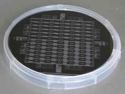
Can you choose wafers for our research? We use the wafers to make molds for PDMS microfluidic devices by soft lithography, and the devices are used for studying bacterial navigation.
Soft Lithography Substrates for PDMS Microfluidic Devices
UniversityWafer supplies silicon wafers, diced silicon substrates, square silicon wafers, fused silica, glass, and ITO-coated substrates for soft lithography, PDMS molding, SU-8 masters, microfluidic chips, Raman reference measurements, SEM analysis, and cleanroom research.
Soft Lithography for Bacterial Navigation Research
An associate research scientist requested help selecting wafers for PDMS microfluidic device fabrication:
Reference #58162 for specs and pricing.
Get Your Soft Lithography Substrate Quote FAST! Or, Buy Online and Start Researching Today!
Diced Silicon Substrates for PDMS Stamps
Silicon is one of the most commonly used master mold materials for soft lithography because it is flat, rigid, cleanroom compatible, and suitable for photolithography, etching, and SU-8 patterning.
A microfluidics researcher requested diced 1 cm × 1 cm silicon substrates etched with microchannels to fabricate a PDMS stamp.
The requested PDMS mold required silicon microchannels approximately 5 µm wide, with spacing from 1 µm to 10 µm and channel depths from 1 µm to 10 µm. The researcher needed 22 diced silicon substrates for microfluidic channel replication.
Reference #243280 for specs and pricing.
Square Silicon Wafers for Soft Lithography
Square silicon wafers are useful for researchers who need non-standard shapes for PDMS molding, lab-on-a-chip development, polymer replication, or custom microfluidic templates.
An electrical engineer requested 4 inch × 4 inch square silicon wafers for soft lithography. UniversityWafer quoted 100 mm × 100 mm P/B <100> silicon, 0.006-0.012 Ω·cm, 525 µm thick, SSP, test grade.
Reference #246314 for more specs and pricing.
Silicon Wafers for Raman and SEM Measurements
Silicon wafers used for soft lithography can also serve as Raman reference substrates and SEM substrates. Researchers often use the same wafer surface to prepare masks, replicate PDMS structures, and perform inspection or characterization.
A chemical engineer requested silicon wafers for soft lithography, PDMS mask preparation, Raman reference measurement, and SEM substrate use.
UniversityWafer supplied 100 mm silicon wafers, Items #447 and #452.
Reference #245500 for specs and pricing.
Common Substrates Used for Soft Lithography
Soft lithography is a microfabrication technique that uses elastomeric molds, stamps, and templates to replicate micron- and nanoscale features. The choice of substrate depends on the desired device, fabrication process, optical requirements, and chemical compatibility. UniversityWafer supplies several materials commonly used for soft lithography, microfluidics, MEMS, and biomedical research.
Popular Soft Lithography Substrates
- Glass Wafers – Excellent optical transparency, chemical resistance, and surface flatness for biosensors, lab-on-a-chip devices, and microscopy.
- Silicon Wafers – The industry standard for fabricating SU-8 masters, PDMS molds, MEMS devices, and microfluidic channels due to their dimensional stability and compatibility with photolithography.
- Polymer Substrates – Materials such as PMMA, PET, and polystyrene provide lightweight, inexpensive solutions for flexible electronics, disposable diagnostic devices, and biomedical applications.
- Metal Substrates – Gold, aluminum, and silver are used when electrical conductivity, plasmonic behavior, or reflective properties are required.
- Hydrogels – Frequently selected for tissue engineering, organ-on-chip devices, drug delivery systems, and cell culture because of their excellent biocompatibility.
The substrate should also be compatible with the elastomer used during replication, most commonly polydimethylsiloxane (PDMS).
Soft Lithography Process
Unlike conventional photolithography, soft lithography relies on flexible PDMS stamps rather than expensive chrome masks. A patterned silicon master is fabricated using photolithography and photoresists such as SU-8. Liquid PDMS is then poured over the master, cured, and peeled away to create an accurate replica of the microstructures.
Because PDMS exhibits excellent chemical resistance, optical transparency, gas permeability, flexibility, and thermal stability, it has become the preferred material for producing reusable molds and stamps.
Applications of Soft Lithography
Soft lithography enables rapid, low-cost fabrication of microscale structures that would otherwise require expensive semiconductor manufacturing processes.
- Microfluidic chips
- Lab-on-a-chip devices
- MEMS fabrication
- Biosensors
- Cell culture platforms
- Tissue engineering
- Drug discovery
- Polymer replication
- Flexible electronics
- Optical devices
Additional fabrication methods include micro-molding in capillaries (MIMIC), microcontact printing, replica molding, and solvent-assisted micromolding.
Researchers' Preferred Silicon Wafers for Soft Lithography
A mechanical engineering professor requested the following substrate for producing PDMS microfluidic devices.
"I'd like a quotation for 76.2 mm P-type <100> SSP silicon wafers (Item #447). We have successfully used these wafers with SU-8 photoresist and Sylgard 184 (PDMS) for fabricating soft lithography masters."
UniversityWafer confirmed that Silicon Item #447 is widely used by university laboratories for fabricating SU-8 masters and PDMS microfluidic molds.
Reference #252195
3-Inch Silicon Wafers for Cleanroom Soft Lithography
A postdoctoral researcher requested polished 3-inch silicon wafers for fabricating SU-8 structures used as PDMS molds in a cleanroom environment.
The wafers were specified as approximately 0.5 mm thick with single-side polishing and were intended for repeated production of microfluidic chips.
Reference #257374
Custom Silicon Templates for Soft Lithography
A university research group requested custom phosphorus-doped silicon wafers approximately 5 cm wide and up to 250 cm long for large-area soft lithography templates.
Initially, test-grade silicon wafers were requested for prototype development before transitioning to prime-grade material for long-term production.
Reference #259168
Fused Silica and ITO for Polymer Replication
Soft lithography is not limited to silicon. Researchers also use fused silica and ITO-coated glass for optical microfluidics, polymer replication, biosensors, and hot embossing processes.
Researchers fabricated microfluidic channel features on silicon, fused silica, and ITO substrates before using them as molds for polymer replication and soft lithography.
Popular Online Items
Reference #ONLQ38615