
What Is Microfabrication?
Microfabrication is a collection of manufacturing processes used to create structures with dimensions ranging from the micrometer scale down into the nanoscale. Originally developed for integrated-circuit manufacturing, microfabrication techniques are now widely used for MEMS, microfluidics, sensors, photonics, biomedical devices, microelectronics, and advanced materials research.
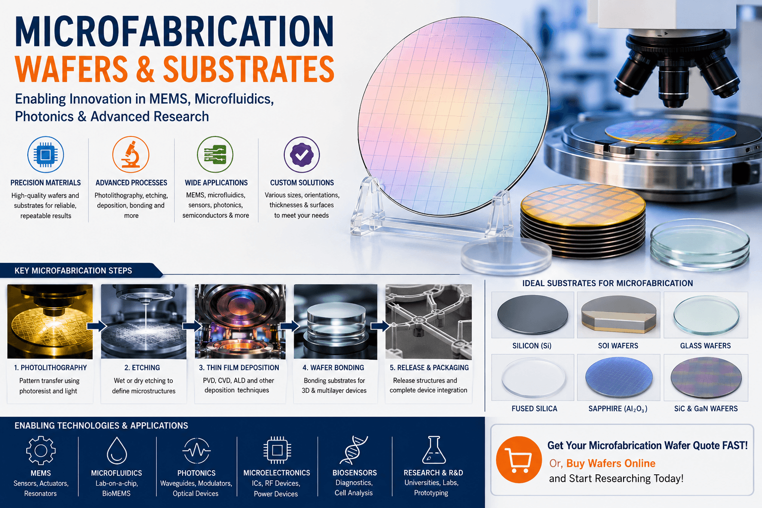
A typical microfabrication process combines multiple techniques rather than relying on a single manufacturing step. Depending on the device, fabrication may involve photolithography , thin-film deposition, wet or dry etching, oxidation, doping, wafer bonding, surface modification, and metallization.
UniversityWafer supplies silicon wafers , silicon-on-insulator (SOI) wafers , glass, fused silica, sapphire, and specialty substrates for microfabrication research, prototyping, and device development.
Silicon Wafers for Microfabrication
Silicon wafers for microfabrication are widely used because high-quality single-crystal silicon provides a flat, dimensionally stable substrate compatible with mature semiconductor processing techniques. Silicon can be patterned using photolithography and etched using both wet chemical and plasma-based processes.
Researchers can select silicon wafers by diameter, crystal orientation, conductivity type, resistivity, thickness, and surface finish. Common options include (100) and (111) silicon, p-type and n-type material, single-side polished (SSP), double-side polished (DSP), and high-resistivity substrates.
The best specification depends on the fabrication process. For example, electrical resistivity may be relatively unimportant when a wafer is used only as a rigid master for polymer replication, but it can become critical when the silicon forms an electrically active part of the finished device.
Photolithography on Silicon Wafers
Photolithography is one of the fundamental pattern-transfer techniques used in microfabrication. A photosensitive material called photoresist is applied to the substrate, typically by spin coating, and then selectively exposed to light through a photomask or by a maskless exposure system.
After development, the patterned resist can serve as a temporary mask for processes such as etching, deposition, ion implantation, or lift-off. Feature size and pattern fidelity depend on the lithography system, exposure wavelength, numerical aperture, photoresist system, mask quality, substrate topography, and process conditions.
Polished silicon is particularly useful for lithography because its smooth, flat surface supports uniform photoresist coating and accurate patterning. Researchers requiring thicker resist structures can also explore silicon wafers for SU-8 photoresist and high-aspect-ratio microfabrication.
Wet and Dry Etching for Microfabrication
After lithographic patterning, selected material can be removed through wet or dry etching. Wet etching uses liquid chemical solutions, while dry etching generally uses reactive plasma species to remove material from exposed regions of the substrate.
Silicon etching can be isotropic or anisotropic depending on the process. In crystalline silicon, alkaline solutions such as KOH and TMAH can exhibit strongly orientation-dependent etch rates. This behavior allows crystal planes to define sidewalls and cavities in MEMS and microfluidic structures.
Dry processes such as reactive ion etching (RIE) provide additional control over feature geometry. Deep reactive ion etching (DRIE) is widely used when deep, high-aspect-ratio silicon structures with relatively vertical sidewalls are required.
SOI Wafers for MEMS Microfabrication
SOI wafers for MEMS are especially useful when the device requires a well-controlled silicon structural layer. A typical SOI wafer consists of a crystalline silicon device layer, a buried silicon dioxide layer known as the buried oxide (BOX), and a silicon handle wafer.
In many SOI MEMS processes, the thickness of the device layer defines the thickness of structures such as beams, resonators, membranes, or proof masses. The BOX can provide electrical isolation and, in suitable etch processes, act as an etch-stop or sacrificial layer.
SOI substrates are used for accelerometers, pressure sensors, microresonators, RF MEMS, BioMEMS, silicon photonics, and other devices requiring precise control of the active or mechanical silicon layer.
Microfluidic Microfabrication
Microfluidic microfabrication uses microscale channels, chambers, valves, membranes, and related structures to manipulate small volumes of liquids or gases. Applications include lab-on-a-chip devices, biosensors, analytical systems, biomedical research, chemical analysis, and organ-on-chip platforms.
Silicon can be directly etched to create microfluidic features or used as a master substrate for polymer replication. Smooth polished wafers are particularly useful when accurate surface replication and controlled microchannel geometry are required.
Soft Lithography and PDMS Microfabrication
Soft lithography is widely used for rapid fabrication of microfluidic and biomedical structures. A common approach begins by patterning a master on a silicon wafer using a thick photoresist such as SU-8.
Liquid polydimethylsiloxane (PDMS) can then be cast over the patterned master, cured, and removed to produce a flexible replica containing the desired microstructures. The replicated PDMS layer can subsequently be bonded to glass, silicon, or another suitable surface to form enclosed microchannels.
Silicon wafers are commonly selected as substrates for PDMS soft lithography because they provide a rigid, flat, cleanroom-compatible surface suitable for photoresist processing and repeated mold replication.
Glass and Fused Silica for Microfabrication
Silicon is not the only substrate used in microfabrication. Glass wafers are useful for microfluidics, sensors, wafer bonding, packaging, and applications where optical transparency or electrical insulation is desirable.
Fused silica wafers provide high optical transparency, low optical absorption over useful wavelength ranges, electrical insulation, and good chemical and thermal stability. These characteristics make fused silica valuable for photonics, optical microdevices, microfluidics, and analytical systems.
Thin-Film Deposition in Microfabrication
Many microfabricated devices contain multiple layers with different electrical, optical, chemical, or mechanical functions. Thin-film deposition can be used to form dielectric, semiconductor, metallic, piezoelectric, or protective layers on a wafer.
Common deposition techniques include physical vapor deposition (PVD), chemical vapor deposition (CVD), atomic layer deposition (ALD) , evaporation, sputtering, and epitaxial growth. The appropriate technique depends on the required material, thickness, conformality, crystallinity, temperature budget, and device architecture.
Wafer Bonding and Multilayer Microdevices
Wafer bonding allows two substrates to be joined to form sealed cavities, multilayer structures, microfluidic channels, MEMS packages, or engineered substrates. Depending on the materials and application, bonding methods can include direct bonding, anodic bonding, adhesive bonding, eutectic bonding, and other approaches.
Silicon-to-glass anodic bonding is particularly useful in selected MEMS and microfluidic applications because it can produce a strong hermetic or near-hermetic interface between suitable silicon and alkali-containing glass substrates under appropriate processing conditions.
Choosing Wafers for Microfabrication
The correct microfabrication substrate depends on the process flow and final device requirements. Important specifications can include:
- Material: silicon, SOI, glass, fused silica, sapphire, or specialty semiconductor
- Diameter: matched to fabrication and cleanroom equipment
- Crystal orientation: important for silicon etching and other orientation-sensitive processes
- Conductivity and resistivity: selected according to electrical requirements
- Thickness: chosen for mechanical strength and device geometry
- Surface finish: SSP, DSP, or application-specific polishing
- Surface roughness: important for lithography, bonding, optics, and thin-film deposition
- TTV, bow, and warp: relevant to lithography, bonding, handling, and process uniformity
- Coatings: oxide, nitride, metals, photoresist, or other functional films when required
Researchers should match these parameters to the complete process rather than selecting a wafer based on material alone. A substrate suitable for a simple SU-8 master, for example, may have very different requirements from an SOI wafer used to fabricate a precision MEMS resonator.
Microfabrication Applications
UniversityWafer substrates can support microfabrication research involving:
- MEMS sensors and actuators
- Microfluidic and lab-on-a-chip devices
- BioMEMS and biomedical research
- Silicon photonics and optical microdevices
- Pressure sensors and accelerometers
- Microresonators and RF MEMS
- Thin-film devices and sensors
- PDMS molds and soft lithography
- Semiconductor device prototyping
- Micro- and nanoscale materials research
Get Your Microfabrication Wafer Quote FAST!
Or, Buy Wafers Online
and Start Researching Today!
Advanced Microfabrication Process Integration
A successful microfabrication process depends on more than performing individual lithography, deposition, and etching steps. Each process must be compatible with the materials and structures already present on the wafer. Temperature limits, chemical compatibility, surface condition, film stress, alignment accuracy, contamination, and wafer geometry can all affect subsequent fabrication steps.
UniversityWafer supplies semiconductor wafers and substrates for developing microfabrication processes ranging from basic test structures to MEMS, photonic, microfluidic, and semiconductor devices.
Photolithography for Microscale Patterning
Photolithography transfers geometric patterns into a photosensitive resist layer. A typical process can include wafer cleaning, dehydration, adhesion promotion, photoresist coating, soft baking, exposure, development, inspection, and subsequent pattern transfer.
Positive photoresists generally become more soluble in developer in exposed regions, while negative resists become less soluble after exposure and appropriate processing. The choice of resist depends on required resolution, film thickness, exposure system, etch resistance, lift-off requirements, and process chemistry.
Feature resolution is influenced by factors including exposure wavelength, numerical aperture, resist chemistry and thickness, focus, mask quality, substrate topography, and process control. Highly polished wafers can help provide uniform resist coating and reproducible lithographic processing.
SU-8 for High-Aspect-Ratio Microstructures
SU-8 photoresist is an epoxy-based negative-tone resist widely used when relatively thick, high-aspect-ratio microstructures are required. Depending on formulation and processing conditions, SU-8 can produce structures ranging from several micrometers to hundreds of micrometers in thickness.
SU-8 is commonly used to fabricate microfluidic masters, molds, channels, pillars, and other MEMS or BioMEMS structures. Silicon wafers are frequently used as SU-8 master substrates because they provide smooth, rigid surfaces compatible with conventional cleanroom processing.
Reactive Ion Etching (RIE)
Reactive ion etching (RIE) is a plasma-based dry etching technique used to transfer lithographically defined patterns into silicon, silicon dioxide, silicon nitride, and many other microfabrication materials. Reactive chemical species participate in material removal while energetic ions can provide directional bombardment of the surface.
By controlling gas chemistry, pressure, plasma power, substrate bias, and temperature, RIE processes can be adjusted for etch rate, selectivity, anisotropy, and sidewall profile. The optimum conditions depend strongly on the material being etched and the masking layer.
Deep Reactive Ion Etching (DRIE) of Silicon
Deep reactive ion etching (DRIE) is widely used for producing deep, high-aspect-ratio structures in silicon. One commonly used implementation is the Bosch process, which alternates between an etching step and a sidewall-passivation step.
This cyclic process can create relatively vertical sidewalls and deep trenches, although characteristic sidewall scalloping can occur. DRIE is important for MEMS accelerometers, gyroscopes, resonators, through-silicon features, microfluidic structures, and other devices requiring deep silicon micromachining.
Crystal orientation is generally less central to DRIE geometry than it is for crystallographically selective wet etching. Researchers interested in orientation-dependent silicon processing can explore silicon wafers for anisotropic etching .
Bulk and Surface Micromachining
Two important approaches to MEMS fabrication are bulk micromachining and surface micromachining. Bulk micromachining forms structures by removing significant portions of the substrate itself. Wet anisotropic etching and DRIE are common methods for creating cavities, membranes, trenches, and other structures in silicon.
Surface micromachining instead constructs structures primarily from thin films deposited and patterned on the substrate. Sacrificial layers can be selectively removed to release movable beams, membranes, resonators, and other mechanical components.
SOI Wafers for Precision MEMS Structures
SOI wafers for MEMS provide a particularly useful platform for defining structures with controlled thickness. The crystalline silicon device layer can become the mechanical structure, while the buried oxide (BOX) separates it from the silicon handle wafer.
During appropriate DRIE processes, the BOX can function as an etch-stop layer. It can also be selectively removed in suitable processes to release portions of the silicon device layer. These capabilities make SOI useful for resonators, inertial sensors, pressure sensors, optical MEMS, and other precision microsystems.
Thin-Film Deposition for Microfabricated Devices
Microfabricated devices frequently require layers that provide electrical conduction, insulation, optical functionality, chemical resistance, piezoelectric response, or mechanical structure. These layers can be formed using several thin-film deposition methods.
Physical vapor deposition techniques such as evaporation and sputtering are widely used for metals and selected dielectric or functional materials. Chemical vapor deposition techniques can produce materials such as silicon dioxide, silicon nitride, polysilicon, and other films depending on the specific chemistry and reactor.
Atomic layer deposition (ALD) is useful when precise thickness control and highly conformal coatings are required. Its sequential, self-limiting surface reactions make ALD particularly valuable for coating certain three-dimensional and high-aspect-ratio microstructures.
Silicon Dioxide in Microfabrication
Thermal oxide on silicon is widely used in microfabrication. Silicon dioxide (SiO₂) can provide electrical insulation, surface passivation, masking, optical functionality, and sacrificial or structural roles depending on the process.
Thermal SiO₂ is formed by oxidizing silicon at elevated temperature in dry oxygen or steam-containing environments. Dry oxidation generally provides slower growth and is often selected for relatively thin, high-quality oxides, while wet oxidation provides substantially faster oxide growth and is commonly used when thicker films are required.
Silicon Nitride for MEMS and Microfabrication
Silicon nitride films are used as dielectric layers, passivation films, oxidation masks, diffusion barriers, optical layers, and mechanical membranes. Their exact properties depend strongly on deposition method and film composition.
LPCVD silicon nitride can provide dense films with useful mechanical and barrier properties, while PECVD processes allow deposition at lower temperatures. Film stress is particularly important for suspended MEMS membranes and other mechanically sensitive microstructures.
Metal Thin Films and Lift-Off Processing
Metals such as aluminum, gold, platinum, titanium, chromium, copper, and others are used in microfabricated devices for electrodes, interconnects, heaters, sensing elements, contact pads, mirrors, and functional coatings. The appropriate metal stack depends on electrical, chemical, mechanical, optical, and thermal requirements.
Lift-off is one method for patterning deposited films. Photoresist is patterned before deposition, the film is deposited over the wafer, and the resist is subsequently removed so that material deposited on top of the resist is lifted away. Appropriate resist profiles and deposition directionality help produce clean pattern definition.
Wafer Bonding for MEMS and Microfluidics
Wafer bonding enables microfabricators to construct multilayer structures, sealed cavities, microchannels, device packages, and engineered substrates. The bonding method must be selected according to the substrate materials, thermal budget, surface condition, required bond strength, and device architecture.
Anodic bonding is commonly used to join silicon to suitable alkali-containing glasses. Elevated temperature and an applied electric field promote ionic redistribution in the glass and formation of a strong interface with silicon.
Direct bonding can join sufficiently smooth, clean surfaces without an intermediate adhesive, although surface preparation and subsequent thermal treatment can strongly affect bond strength. Adhesive and metal-based bonding methods are alternatives when process requirements favor lower temperatures or different materials.
Microfabrication for Silicon Photonics
Microfabrication techniques are also essential for silicon photonics. Optical waveguides, resonators, couplers, modulators, and related structures can be patterned into semiconductor materials using high-resolution lithography and controlled etching.
Silicon-on-insulator wafers are widely used for silicon photonics because the refractive-index contrast between the silicon device layer and buried SiO₂ enables strong optical confinement in appropriately designed waveguides.
Microfabrication for Sensors and BioMEMS
Microfabrication enables compact sensors that respond to pressure, acceleration, temperature, chemical species, biological interactions, light, and other physical quantities. Devices may combine mechanical, electrical, optical, and fluidic functions on the same substrate or within a bonded microsystem.
Microfluidic microfabrication is particularly important for BioMEMS, lab-on-a-chip systems, biosensors, cell-analysis platforms, and chemical assays where precise manipulation of small liquid volumes is required.
Wafer Surface Quality and Microfabrication Yield
Surface quality can directly influence lithography, deposition, bonding, optical performance, and device reliability. Particles, scratches, contamination, excessive roughness, and poor wafer geometry can introduce defects or reduce process uniformity.
Chemical mechanical polishing (CMP) can be used to produce highly planar surfaces and is an important process in both substrate preparation and multilayer semiconductor fabrication.
For processes involving wafer bonding, advanced lithography, or optical structures, parameters such as surface roughness, total thickness variation (TTV), bow, and warp may require tighter control than for basic proof-of-concept experiments.
Cleanroom Contamination Control
Microfabrication is commonly performed in controlled cleanroom environments because small particles and trace contaminants can interfere with lithography, film growth, etching, bonding, and device performance. Requirements become increasingly stringent as feature dimensions decrease or device sensitivity increases.
Cleaning procedures depend on the substrate and process. Semiconductor fabrication may use combinations of solvent cleaning, aqueous chemical cleaning, plasma treatment, UV-ozone treatment, or other surface-preparation methods. A cleaning method suitable for bare silicon may not be appropriate for a wafer containing metals, polymers, compound semiconductors, or sensitive thin films.
Microfabrication Metrology and Process Control
Reliable microfabrication requires measurement throughout the process. Optical microscopy can inspect patterns and defects, while profilometry can measure step height and surface topography. Ellipsometry and reflectometry are commonly used for thin-film characterization, and atomic force microscopy (AFM) can provide nanoscale surface-topography information.
Researchers interested in high-resolution surface characterization can explore atomic force microscopy on silicon wafers . Selecting the appropriate metrology method helps verify critical dimensions, film thickness, roughness, etch depth, and other process parameters.
Selecting Substrates for Your Microfabrication Process
There is no single ideal microfabrication wafer for every application. The substrate should be selected according to the complete fabrication sequence and the electrical, mechanical, optical, thermal, and chemical requirements of the finished device.
Before ordering wafers, consider specifying:
- Substrate material: silicon, SOI, glass, fused silica, sapphire, or specialty semiconductor
- Wafer diameter: compatible with lithography, deposition, etching, and handling equipment
- Crystal orientation: particularly important for anisotropic silicon etching
- Dopant and conductivity type: when the substrate participates electrically in the device
- Resistivity: matched to RF, detector, MEMS, or electronic requirements
- Thickness: selected for mechanical and process requirements
- Surface finish: SSP, DSP, or application-specific polishing
- Surface roughness: especially important for bonding, optics, and thin-film growth
- TTV, bow, and warp: important for process uniformity, lithography, and wafer bonding
- Surface layers: SiO₂, Si₃N₄, metals, photoresist, or other coatings when required
UniversityWafer supplies semiconductor and microfabrication wafers for MEMS, microfluidics, photonics, sensors, semiconductor processing, university research, industrial R&D, and prototype fabrication.
Related Microfabrication Resources
- Photolithography Process – Learn how photoresist coating, exposure, development, and pattern transfer are used in semiconductor and MEMS microfabrication.
- SOI Wafers for MEMS – Explore silicon-on-insulator substrates for MEMS sensors, resonators, actuators, and precision micromachining.
- Microfluidic Microfabrication – Wafers and fabrication techniques for microchannels, lab-on-a-chip devices, BioMEMS, and microfluidic research.
- Soft Lithography – Learn about PDMS molding, microfluidic masters, and soft-lithography techniques using silicon and other substrates.
- SU-8 Photoresist Wafers – Silicon substrates for thick SU-8 photoresist, high-aspect-ratio structures, MEMS, and microfluidic mold fabrication.
- Silicon Wafers for Anisotropic Etching – Explore crystallographic silicon etching for MEMS cavities, channels, membranes, and other microstructures.
- Silicon-on-Insulator (SOI) Wafers – Engineered substrates with a silicon device layer and buried oxide for MEMS, photonics, sensors, and microelectronics.
- Atomic Layer Deposition (ALD) – Learn about precise and conformal thin-film deposition for microfabricated devices and high-aspect-ratio structures.
- Silicon Nitride (Si₃N₄) Wafers – Silicon nitride materials and coated wafers for membranes, dielectric layers, passivation, optics, and MEMS.
- Chemical Mechanical Polishing (CMP) – Explore wafer planarization and surface preparation for lithography, bonding, deposition, and semiconductor processing.
- Glass Wafers – Glass substrates for microfluidics, MEMS, sensors, optical devices, wafer bonding, and microfabrication.