
Essential Points About Plasmonics and Photonics Wafers
- Silicon wafers serve as primary substrates for both photonic and plasmonic applications
- Thermal oxide silicon wafers are crucial for optical waveguide fabrication
- Gallium Nitride on Silicon provides enhanced performance for photonic devices
- Lithium Niobate (LiNbO3) wafers offer excellent electro-optic properties
- Hydrophobic coatings can modify surface properties for specialized applications
- Single crystal quartz wafers are valuable for specific photonic implementations
- Integration of plasmonic and photonic structures enhances device functionality
- Material selection significantly impacts light manipulation capabilities
Get Your Quote FAST! Or, Buy Online and Start Your Research Today!
Introduction to Plasmonics and Photonics
Plasmonics and photonics represent two exciting areas in materials science and optical technology. Photonics involves generating, controlling, and detecting light waves and photons, while plasmonics studies how electromagnetic fields interact with free electrons in metals. These fields are changing how we think about manipulating light at very small scales.
When plasmonic and photonic technologies work together, they enable remarkable advances in fields from telecommunications to medical diagnostics. These technologies let scientists manipulate light at scales much smaller than the wavelength of light itself, opening new possibilities for tiny optical devices and sensors.
The foundation of both photonics and plasmonics research is the substrate materials used. Silicon wafers serve as the main platform for many applications, but specialized substrates like Gallium Nitride on Silicon and Lithium Niobate offer unique properties that enhance specific photonic and plasmonic functions.
Understanding Plasmonics: Fundamentals and Applications
Plasmonics is a rapidly growing field that explores what happens when light interacts with free electrons at metal surfaces. These interactions create surface plasmon polaritons (SPPs) - electromagnetic waves that travel along the boundary between metals and dielectrics (non-conducting materials).
What is Plasmonics?
Plasmonics focuses on surface plasmons, which are collective oscillations of free electrons at metal surfaces. These oscillations can concentrate light into extremely small volumes, creating intense electromagnetic fields. This concentration effect makes possible applications ranging from enhanced spectroscopy to ultra-sensitive biosensors.
Plasmonics bridges the gap between photonics and electronics. It allows for devices that operate at optical frequencies (the speed of light) but with dimensions comparable to electronic components (nanoscale). This makes plasmonic devices promising candidates for next-generation integrated circuits that combine the speed of photonics with the small size of electronics.
Substrates for Plasmonics Research
The choice of substrate is critical for plasmonic applications. While the plasmonic materials themselves are typically noble metals like gold and silver, the substrate upon which these metals are deposited plays a crucial role in determining how well plasmonic devices perform.
Silicon wafers work exceptionally well as platforms for plasmonic research because of their well-established fabrication processes and compatibility with existing semiconductor technologies. Thermal oxide silicon wafers are particularly valuable because they provide an insulating layer that can enhance plasmonic effects.
For specialized plasmonic applications, researchers often use alternative substrates. Single crystal quartz wafers offer excellent optical transparency and thermal stability, making them suitable for high-temperature plasmonic applications. Meanwhile, hydrophobic silicon wafers with special coatings provide unique surface properties that can be advantageous for certain plasmonic sensors.
Photonics: Light-Based Technologies and Materials
Photonics is the science and technology of generating, controlling, and detecting photons (particles of light). Unlike electronics which uses electrons to carry information, photonics uses light, offering advantages in bandwidth, speed, and energy efficiency.
Fundamentals of Photonic Devices
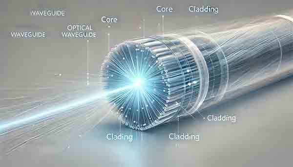
Photonic devices manipulate light for various applications, from telecommunications to sensing. The core components of photonic systems include waveguides, resonators, modulators, and detectors. These components rely on high-quality substrate materials with precise optical properties.

Optical waveguides are particularly important in photonic systems, serving as the "wires" that guide light between different components. Silicon waveguides have become the standard in integrated photonics due to their compatibility with CMOS fabrication processes. Silicon-based optical waveguides can be created through careful etching and deposition processes on high-quality silicon wafers.
Substrates for Photonic Devices
Choosing the right substrates is crucial for photonic device performance. At UniversityWafer, a range of materials is available optimized for different photonic applications:
Silicon Wafers: These form the foundation of most photonic integrated circuits. Silicon offers excellent mechanical stability and compatibility with established fabrication techniques.
Thermal Oxide Silicon Wafers: The oxide layer provides optical isolation and can serve as part of the waveguide structure. Thick thermal oxide layers are particularly valuable for photonic applications.
Gallium Nitride on Silicon: This combination offers enhanced performance for optoelectronic devices, particularly those operating at blue and ultraviolet wavelengths. GaN on Si wafers provide high uniformity and lower leakage current, making them ideal for high-performance photonic applications.
Lithium Niobate (LiNbO3): Known for its excellent electro-optic properties, lithium niobate wafers are essential for creating optical modulators and switches in photonic systems.
Silicon Wafers for Plasmonics and Photonics
Silicon wafers form the backbone of both photonic and plasmonic device fabrication. Their widespread use comes from the mature manufacturing ecosystem, well-understood material properties, and compatibility with existing semiconductor fabrication facilities.
Silicon in Photonic Applications
In photonic applications, silicon serves as both a structural and functional material. Silicon's high refractive index allows for strong light confinement in waveguides, while its transparency at telecommunications wavelengths (1.3-1.6 μm) makes it ideal for optical communications applications.
Silicon photonics has emerged as a leading technology for integrated optical circuits, enabling the creation of complex systems including optical transceivers, modulators, and sensors on a single chip. High-quality silicon wafers with precise specifications are essential for achieving the performance required in these advanced applications.
Silicon in Plasmonic Applications
While silicon itself is not a plasmonic material (as it lacks free electrons), silicon wafers serve as excellent substrates for plasmonic structures. Typically, plasmonic materials like gold or silver are deposited onto silicon wafers, which provide mechanical support and integration with other components.
Silicon's compatibility with standard fabrication processes makes it particularly valuable for creating hybrid photonic-plasmonic devices. These hybrid systems leverage the advantages of both technologies: the low loss and long propagation distances of photonics combined with the strong field confinement of plasmonics.
Thermal Oxide Silicon Wafers
Thermal oxide silicon wafers feature a layer of SiO2 grown through thermal oxidation. This oxide layer serves multiple functions in photonic and plasmonic applications:
- Optical Isolation: The oxide layer can isolate optical modes from the silicon substrate, reducing losses.
- Waveguide Formation: In some designs, the oxide layer forms part of the waveguide structure.
- Surface Passivation: The oxide provides a stable surface for subsequent processing steps.
The thickness of the thermal oxide layer can be precisely controlled, allowing researchers to tailor the optical properties of their devices. At UniversityWafer, thermal oxide silicon wafers are used in research for applications including ultrafast XUV spectroscopy with enhanced surface sensitivity.
Advanced Materials for Photonic and Plasmonic Applications
While silicon remains the dominant material in integrated photonics and plasmonics, several specialized materials offer unique advantages for specific applications.
Gallium Nitride on Silicon
Gallium Nitride (GaN) on Silicon combines the excellent optical properties of GaN with the mechanical and economic advantages of silicon substrates. This material system is particularly valuable for applications in the blue and ultraviolet spectral regions.
GaN on Si wafers offer several advantages for photonic and plasmonic applications:
- High uniformity across the wafer
- Low leakage current for improved device performance
- Higher operating temperatures than pure silicon
- Excellent optical properties in the visible and UV range
These properties make GaN on Si an excellent choice for applications including LED development, high-frequency electronics, and power devices.
Lithium Niobate (LiNbO3) Wafers
Lithium Niobate is a ferroelectric material with exceptional electro-optic, piezoelectric, and nonlinear optical properties. These characteristics make it invaluable for applications requiring high-speed modulation of light.
Lithium Niobate wafers are available in different crystal orientations, each optimized for specific applications:
- X-cut wafers for surface acoustic wave devices
- Y-cut wafers for electro-optic modulators
- Z-cut wafers for nonlinear optical applications
The combination of lithium niobate's unique properties with precise wafer fabrication techniques enables the creation of high-performance photonic devices including modulators, switches, and frequency converters.
Single Crystal Quartz Wafers
Quartz is a crystalline form of silicon dioxide (SiO2) with excellent optical and mechanical properties. Single crystal quartz wafers offer several advantages for specialized photonic applications:
- Exceptional optical transparency across a wide spectral range
- High thermal stability
- Excellent mechanical strength
- Natural birefringence useful for polarization control
These wafers are available in various cuts, including X, Y, Z, AT, and ST cuts, each optimized for different applications. Quartz wafers find applications in electronic devices, medical instruments, and specialized photonic components where their unique properties offer advantages over standard silicon.
Hydrophobic Silicon Wafers
For applications requiring specific surface properties, hydrophobic silicon wafers with Teflon coatings provide an excellent solution. These wafers feature a high contact angle that repels water and other polar substances.
The hydrophobic properties make these wafers particularly valuable for:
- Microfluidic devices where controlled wetting is crucial
- Self-cleaning surfaces in optical applications
- Specialized plasmonic sensors where surface chemistry plays a role
- Research into surface-enhanced spectroscopy techniques
These wafers are typically available as single-sided polished with standard thickness, providing researchers with a reliable platform for developing advanced photonic and plasmonic devices with specialized surface requirements.
Fabrication Techniques for Photonic and Plasmonic Devices
Creating photonic and plasmonic devices requires sophisticated fabrication techniques that can achieve the necessary precision at nanoscale dimensions. Understanding these processes is essential for researchers working in these fields.
Wafer Fabrication Processes
The foundation of photonic and plasmonic device fabrication lies in high-quality wafer processing. Silicon wafer fabrication involves multiple steps, from crystal growth to final polishing.

Key processes in wafer fabrication include:
- Crystal Growth: Creating the initial silicon ingot through methods like Czochralski (CZ) or Float-Zone (FZ) growth.
- Wafer Slicing: Cutting the ingot into thin wafers, typically resulting in about 30% of silicon being lost as kerf waste.
- Edge Rounding: Smoothing the edges to prevent chipping during processing.
- Lapping and Etching: Removing saw damage and creating a flat surface.
- Polishing: Achieving the mirror-like finish required for photonic applications.
- Cleaning: Removing contaminants that could affect device performance.
These processes establish the foundation upon which photonic and plasmonic structures are built.
Photonic Device Fabrication
The fabrication of photonic devices typically involves several specialized processes:
- Lithography: Patterns are defined using techniques like photolithography or electron-beam lithography, with the latter offering higher resolution necessary for many photonic structures.
- Etching: The pattern is transferred to the substrate through processes like reactive ion etching (RIE) or deep reactive ion etching (DRIE).
- Deposition: Additional materials are added through techniques such as chemical vapor deposition (CVD), physical vapor deposition (PVD), or atomic layer deposition (ALD).
- Thermal Oxidation: For thermal oxide silicon wafers, precise control of the oxidation process is critical to achieving the desired oxide thickness and quality.
Plasmonic Device Fabrication
Plasmonic devices often require additional specialized fabrication steps:
- Metal Deposition: Plasmonic materials (typically gold or silver) are deposited through techniques like evaporation or sputtering.
- Lift-off Processes: For creating patterned metal structures without etching the metal directly.
- Surface Functionalization: Modifying the surface properties, as in hydrophobic silicon wafers, to enhance specific plasmonic effects or enable particular applications.
The precision required for plasmonic fabrication is often at the nanometer scale, necessitating advanced equipment and carefully controlled processes.
Applications of Photonic and Plasmonic Technologies
The unique capabilities of photonic and plasmonic devices have led to applications across numerous fields, from telecommunications to medical diagnostics.
Optical Waveguides and Integrated Photonics
Optical waveguides form the foundation of integrated photonic circuits, guiding light between different components. Silicon-based optical waveguides have become the standard for photonic integrated circuits due to their compatibility with existing semiconductor manufacturing processes.
These waveguides enable the creation of complex photonic systems including:
- Optical Transceivers: For high-speed data transmission in telecommunications and data centers.
- Optical Sensors: Leveraging the interaction between light and matter for sensitive detection of chemicals, biological materials, or physical parameters.
- Optical Computing: Using light rather than electrons for certain computational tasks, potentially offering higher speed and lower power consumption.
Thick thermal oxide silicon wafers are particularly valuable for waveguide formation, as the oxide layer can serve as part of the waveguide structure or as cladding to confine light within the waveguide.
Plasmonic Sensing and Imaging
Plasmonics enables unprecedented sensitivity in sensing applications due to the strong field enhancement near metallic structures. This has led to numerous applications:
- Surface Plasmon Resonance (SPR) Sensors: Used for label-free detection of biomolecules, these sensors can detect minute changes in refractive index near metal surfaces.
- Surface-Enhanced Raman Spectroscopy (SERS): The enhanced electromagnetic fields near plasmonic structures dramatically increase Raman scattering signals, enabling detection of single molecules.
- Plasmonic Imaging: Beyond the diffraction limit, providing super-resolution imaging capabilities for biological and material science applications.
Hydrophobic silicon wafers with specialized coatings can enhance the performance of plasmonic sensors by controlling surface interactions with analytes.
Conclusion
Plasmonics and photonics represent two of the most exciting frontiers in optical science and technology. The integration of these fields is enabling unprecedented control over light at the nanoscale, opening new possibilities for applications ranging from telecommunications to medical diagnostics.
The choice of substrate material is critical for both photonic and plasmonic applications. While silicon remains the dominant platform due to its compatibility with established fabrication processes, specialized materials like Gallium Nitride on Silicon, Lithium Niobate, and single crystal quartz offer unique advantages for specific applications.
As research in these fields continues to advance, we can expect to see even greater integration of photonic and plasmonic technologies, leading to devices that combine the best features of both approaches. This integration will enable new applications in areas such as quantum information processing, ultra-sensitive sensing, and high-speed optical communications.
For researchers working in these fields, having access to high-quality substrates with precisely controlled properties is essential. At UniversityWafer, we provide a wide range of wafers and substrates optimized for photonic and plasmonic applications, enabling researchers to push the boundaries of what's possible in these exciting fields.