
We would like information on your InGaN inventory, pricing, and specifications. We are interested in InGaN multiple quantum wells for LED structures and require eight devices.
InGaN Multiple Quantum Wells for LEDs and Optoelectronics
A doctoral researcher requested information regarding indium gallium nitride (InGaN) structures for multiple quantum well (MQW) devices used in light-emitting diodes.
Multiple quantum well (MQW) structures based on InGaN/GaN are widely used in blue, green, and ultraviolet LEDs, laser diodes, and photonic devices. Their high radiative efficiency and tunable emission wavelengths make them essential for next-generation optoelectronic applications.
Reference #88298 for specifications and pricing.
Get Your Quote FAST! Or Buy Online Here and Start Researching Today!
P-GaN / Quantum Well / N-GaN Epitaxial Structures
A scientist developing GaN LEDs and GaN-based field-effect transistors requested pricing for 4-inch GaN epitaxial wafers grown on sapphire substrates.
We would like pricing information for 4-inch gallium nitride epitaxy wafers on sapphire. The desired structure is P-GaN / Quantum Well / N-GaN.
UniversityWafer, Inc. quoted the following research-grade GaN epi structures:
| Wafer Type | Specification |
|---|---|
| 100mm GaN Epi-Wafer | C-Plane FSS Sapphire with 4.0 µm GaN epitaxial layer and 650 µm substrate thickness. |
| 100mm GaN Epi-Wafer | C-Plane PSS Sapphire with 6.0 µm GaN epitaxial layer and 650 µm substrate thickness. |
Reference #176462 for additional specifications and pricing.
GaAs and InGaAs Quantum Well Structures
A researcher requested custom semiconductor wafers for fabricating quantum well devices based on gallium arsenide and indium gallium arsenide layers.
I am looking for wafers with the following structure: Top layer: GaAs; Quantum well layer: InGaAs; Spacer layers: GaAs; Bragg reflector: AlAs/GaAs quarter-wave stack; Wafer: Semi-insulating GaAs.
GaAs/InGaAs quantum wells are commonly used in semiconductor lasers, VCSELs, photodetectors, optical communications, and quantum photonic devices. High-quality semi-insulating GaAs substrates provide excellent lattice matching and low defect density for advanced epitaxial growth.
Bragg reflector structures composed of alternating AlAs/GaAs layers are frequently incorporated into vertical-cavity surface-emitting lasers (VCSELs) and resonant cavity devices to enhance optical confinement and improve efficiency.
Reference #192945 for specifications and pricing.
What Are Quantum Wells?
Quantum wells are nanometer-scale semiconductor structures that confine electrons or holes in one direction while allowing movement in the other two directions. This confinement creates discrete energy levels, making quantum wells important for optoelectronic devices, semiconductor lasers, LEDs, solar cells, and high-speed transistors.
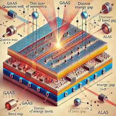 A quantum well is usually fabricated by placing a thin semiconductor layer between two materials with a larger bandgap. For example, GaAs/AlGaAs, InGaAs/InP, and GaN/InGaN structures are commonly used in advanced photonic and electronic research.
Why Quantum Wells Are Important
Quantum wells allow researchers to control the optical and electrical properties of semiconductor devices by adjusting the thickness, composition, and bandgap of each layer. This makes them useful for applications that require precise wavelength emission, high carrier mobility, and improved energy efficiency.
- Semiconductor lasers: Quantum wells help produce narrow, intense light for optical communications, barcode scanners, sensors, and laser diodes.
- LEDs: InGaN quantum wells are widely used in blue and green LED structures.
- HEMTs: Quantum well structures improve carrier mobility in high-electron-mobility transistors for RF and microwave devices.
- Solar cells: Quantum wells can improve light absorption and carrier collection in advanced photovoltaic devices.
- Photodetectors: Quantum well structures are used in infrared detectors and other optoelectronic sensors.
How Quantum Wells Are Fabricated
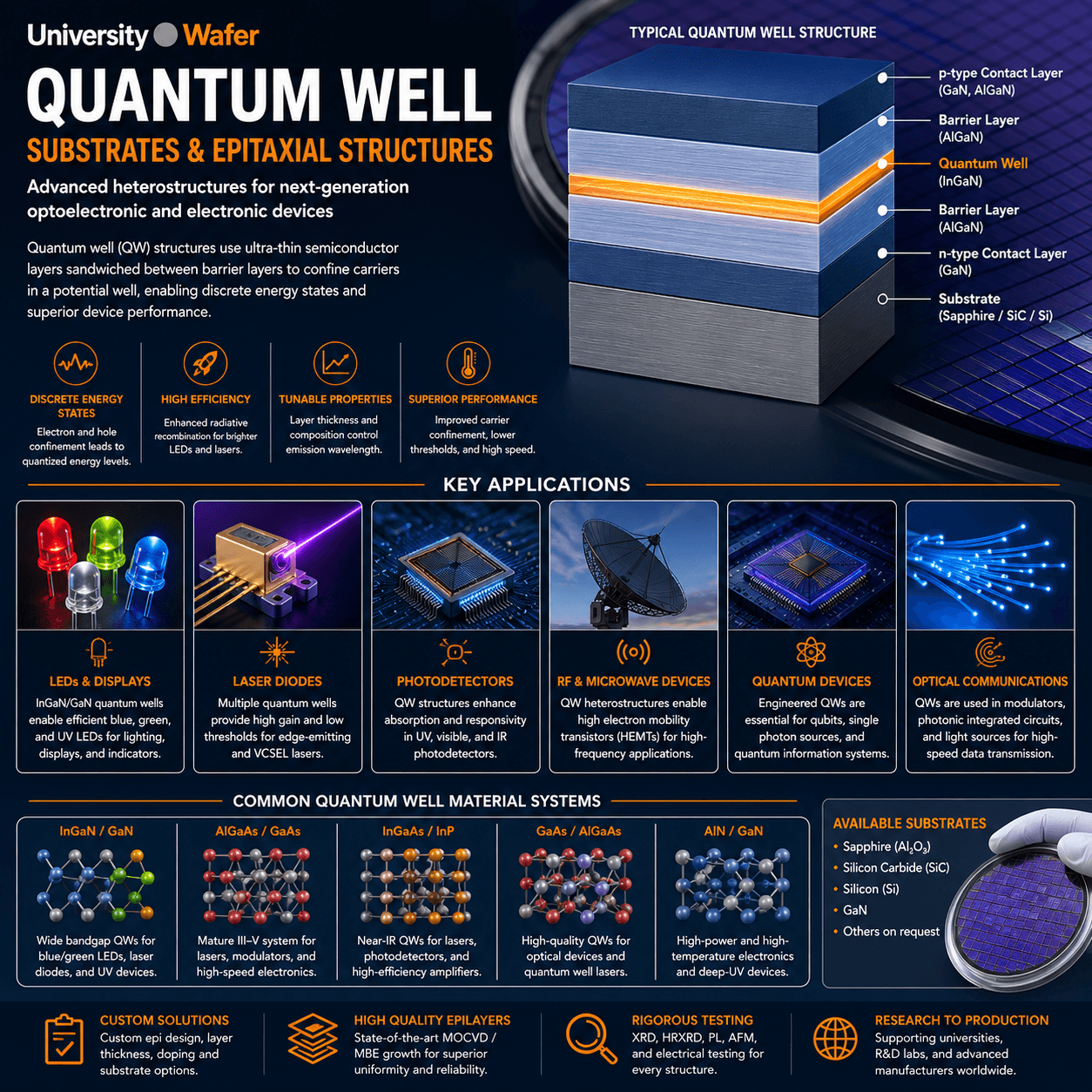
Quantum wells require precise control of semiconductor layer thickness and composition. They are commonly fabricated using molecular beam epitaxy (MBE) or metal-organic chemical vapor deposition (MOCVD). These deposition methods allow researchers to grow high-quality epitaxial layers with carefully controlled bandgap profiles.
Important fabrication requirements include lattice matching, low defect density, clean interfaces, controlled doping, and accurate layer thickness. Even small changes in the quantum well thickness can shift the optical emission wavelength or affect device performance.
Substrates Used to Fabricate Quantum Wells
The substrate material is selected based on the quantum well structure, lattice constant, thermal conductivity, and final device application. Common quantum well substrates include:
- Gallium Arsenide (GaAs): Used for GaAs/AlGaAs and InGaAs quantum wells in lasers, photodetectors, and high-speed electronics.
- Silicon (Si): Used for Si/SiGe quantum wells and integration with CMOS-compatible semiconductor devices.
- Sapphire (Al2O3): Common for GaN/InGaN quantum well LEDs and nitride semiconductor research.
- Indium Phosphide (InP): Used for InGaAs/InP and InGaAsP/InP quantum wells for long-wavelength optoelectronic devices.
- Silicon Carbide (SiC): Used for GaN/AlGaN quantum well structures requiring high thermal conductivity and power handling.
- Zinc Selenide (ZnSe): Used for II-VI quantum wells such as ZnSe/CdSe for visible optoelectronic applications.
- Germanium (Ge): Used in SiGe and high-speed semiconductor research where lattice compatibility is important.
Quantum Well Material Systems
Different semiconductor combinations are selected depending on the wavelength, bandgap, and device requirements. Popular quantum well material systems include:
- GaAs/AlGaAs: Used for lasers, detectors, and high-mobility electronic devices.
- InGaAs/GaAs: Used for near-infrared lasers and photonic devices.
- InGaAs/InP: Used for long-wavelength optical communications and telecom devices.
- GaN/InGaN: Used for blue and green LEDs and nitride-based laser diodes.
- Si/SiGe: Used for CMOS-compatible electronics and high-speed transistor research.
UniversityWafer, Inc. supplies semiconductor wafers and custom substrates used for quantum well fabrication, including GaAs, GaN on sapphire, InGaN, InP, SiGe, silicon, sapphire, SiC, ZnSe, and germanium wafers.
Related Semiconductor Materials and Quantum Well Resources
- Gallium Arsenide (GaAs)
- Indium Gallium Nitride (InGaN)
- Gallium Nitride Epitaxial Wafers
- HEMT Structures
- Molecular Beam Epitaxy (MBE)
- Metal Organic Chemical Vapor Deposition (MOCVD)
- Indium Phosphide (InP)
- Optoelectronic Devices
- Photonic Devices
- Solar Cells
- Silicon Germanium (SiGe)
- Silicon Carbide (SiC)