Fabricating Schottky Diodes
A PhD candidate requested a quote for the following.
My lab is researching MEMS and semiconductor fabrication. I looked up on your website and found that you deal with the various kinds of wafers and depositions.
- Do you also customize the wafers as per the need?
- Do you also, supply diamond wafers? Yes!
One of our clients requires the diamond wafers for the fabrication of a Schottky diode. They need in-situ doped diamond material.
Below are the specifications and requirements for the wafers:
- We need a single crystal CVD diamond material wafers of dimensions between 3x3mm to 8x8mm.
- We need the p+ doping concentration in the wafers of around 1.9x10^20 cm^-3 to 2.1x10^20 cm^-3.
- The p- doping concentration should be in between 1.7x10^15 cm^-3 to 1.9x10^15 cm^-3.
- For the oxide layer, we need the Al2O3 material of thickness around 0.2 to 1um. These are some general specifications of the types of in-situ doped diamond wafers we want. If you have the diamond wafers of such concentrations at your disposal, then kindly send me the price quotation for the wafers. Look forward to hear from you.
Reference #278949 for specs and pricing.
Get Your Quote FAST! Buy Online and Start Researching Today!
What are Structure of Schottky Barrier diodes?
A Schottky barrier diode is a metal–semiconductor junction device rather than a p–n junction diode. Its structure is intentionally simple to achieve fast switching, low forward voltage drop, and low power loss.

1. Basic Physical Structure
A Schottky diode consists of:
A. Metal Contact (Schottky Metal)
Common metals:
The choice of metal affects:
-
Barrier height (Φ_B)
-
Reverse leakage current
-
Forward voltage drop
B. Semiconductor Layer
Usually n-type silicon, but can also be:
Why n-type?
The semiconductor stack often includes:
C. Ohmic Contact (Backside Metal)
The backside (bottom) of the semiconductor has a low-resistance ohmic metal contact, often:
D. Passivation & Guard Ring (for high-voltage SBDs)
To reduce surface leakage and edge breakdown, many SBDs include:
These improve:
2. Cross-Sectional Structure
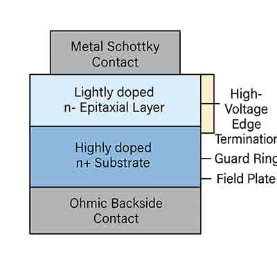
A simplified cross-section:
Metal (Schottky Contact) ------------------------ Lightly Doped n- Epitaxial Layer ------------------------ Heavily Doped n+ Substrate ------------------------ Ohmic Contact (Back Metal)
Edge termination (for high-voltage devices):
Metal Contact | Field Plate -------------|------------ Guard Ring / Junction Termination Extension (JTE)
3. How the Structure Creates the "Schottky Barrier"
When the metal touches the n-type semiconductor, electrons cannot freely flow because of:
This creates:
-
Forward conduction through majority carriers (electrons)
-
No charge storage → fast switching
-
Low forward voltage (~0.2–0.4 V)
Energy band diagram:
4. Variations in Schottky Diode Structures
A. Planar Schottky Diode
B. Trench Schottky (Super Barrier / TMBS)
C. GaN and SiC Schottky Diodes
High-power applications use wide-bandgap semiconductors:
These offer:
5. Key Structural Advantages
| Feature |
Structural Reason |
| Fast switching |
No minority carrier storage (metal–semiconductor junction) |
| Low forward voltage drop |
Low Schottky barrier height (depends on metal) |
| High-speed power electronics |
Simple structure with majority carriers |
| Low reverse recovery time |
No charge storage region like p–n diodes |
Summary
A Schottky diode is built from:
-
Metal Schottky contact
-
Lightly doped n-type epitaxial layer
-
Heavily doped n+ substrate
-
Backside ohmic contact
-
(Optional) Guard rings, field plates, trench structures
This structure creates a metal-semiconductor rectifying junction that allows ultra-fast switching and low forward voltage.

