
Diamond Wafer Applications
A diamond wafer is an ideal material for semiconductor power devices. Its thermal conductivity is higher than the typical silicon wafer, allowing it to be used as a heatsink. A diamond wire-cut chip can be directly inserted into a MEMS foundry process. Its thermal properties allow it to perform well in a variety of applications. There are two main types of a diamond wire-cutted wafer.
DLC Coating on Silicon
Scientist:
UniversityWafer, Inc. Quoted:
DLC coating on Silicon Wafer
150 mm diameter, SSP, doping: N or P-type, prime grade, <100> conventional Ori with a single flat 57.5mm, thickness: 500-700 microns,Chemical Vapor deposition with a 50-100 nm thick Polycrystalline diamond-like carbon (DLC) coating,smooth surface roughness <10nm,uniformity <5%
Get Your Quote FAST! Or, Buy Online and Start Researching Today!
Scratch Test for DLC Coated Silicon Wafer
Video: Learn about Diamond Substrates
Diamond Diced Wafers
We are working with firms that have made gains capturing carbon from the atmosphere and turning into diamonds. Contact us for more info.

What are the Benefits of Using Diamond Wafers?
Diamond wafers have several benefits due to their unique properties, which make them ideal for use in a variety of applications, including electronics, optics, and more. Some of the benefits of using diamond wafers are:
-
High thermal conductivity: Diamond has the highest thermal conductivity of any known material, making it ideal for use in high-power electronic devices, such as high-frequency transistors, where heat dissipation is critical.
-
Hardness and durability: Diamond is the hardest known material, making it extremely resistant to wear and damage. This makes diamond wafers ideal for use in cutting tools, such as saw blades, drills, and machining tools.
-
Optical properties: Diamond has unique optical properties, including high transparency across a wide range of wavelengths, making it ideal for use in optical windows, lenses, and other optical components.
-
Chemical inertness: Diamond is highly resistant to chemical corrosion and does not react with most chemicals. This property makes diamond wafers ideal for use in harsh chemical environments, such as in chemical processing plants.
-
Biocompatibility: Diamond is biocompatible, meaning it is not harmful to living tissue. This property makes diamond wafers ideal for use in medical devices, such as surgical tools and implants.
Overall, the unique properties of diamond wafers make them highly desirable for use in a wide range of applications, including those that require high thermal conductivity, durability, optical transparency, chemical inertness, and biocompatibility.
Related Substrates & Materials
- Silicon Wafers (base substrate for DLC coatings)
- Silicon Carbide (SiC) Wafers (power electronics substrates)
- GaN on Sapphire (high-frequency / high-power devices)
- AlGaN/GaN on Sapphire
- Thermal Oxide on Silicon (process-ready silicon options)
- Silicon-on-Insulator (SOI) (MEMS and RF platforms)
- Graphene Substrates (advanced coatings & electronics R&D)
- 150 mm Silicon Wafers (6-inch diameter, popular for coating requests)
- Contact Us (send specs for a quote)
What Is a Diamond Wafer?
A diamond wafer is a small, thin piece of material made of pure diamond. It is used in semiconductor production. However, because the diameter of a standard diamond wafer is only 75 mm, it is not practical to produce them in large quantities. Therefore, industrial research and development needs larger diameter wafers. The process of growing a diamond is time consuming, but if done correctly, the process can be completed in a single day.
The size and shape of a diamond wafer depends on its application. The diamond single  crystal wafer is one of the most popular types of semiconductors. It can be found in various shapes and sizes, ranging from 10x10mm to 4" diameter. The size of the diamond wafer depends on its application. It can be used for tribological testing, MEMS development, and unique nano-scale processing.
In the electronics industry, it is possible to make a diamond wafer using a variety of innovative growth techniques. These include chemical vapor deposition energized with a microwave source, and thermodynamic growth under high pressure. But the technique is slow and complicated. In the end, a single crystal diamond wafer is a valuable commodity that can replace silicon components in electronics. So, what exactly is a diamond-wafer?
Despite the complexity of diamond technology, its high performance is a desirable attribute for many applications. The high degree of surface roughness allows diamond to conduct electricity at high voltages. Its low surface temperature makes it a popular material for semiconductors and other surfaces in the electronics industry. The process also reduces carbon input in the production of these semiconductors. And because the diamond is so hard, it can be used in heat sinks.
In semiconductor manufacturing, a diamond wafer is used in many applications. It is a semiconductor material that has a high thermal conductivity. Its thermal conductivity can reach 2000 W/cmK. It is the most common material for heatspreaders and heatsinks. The diamond wire cut wafers are more efficient. They can also be used for electrical isolation or stress relieving slits.
It can also be used for experimental purposes. A diamond wire wafer is a good example of this. Its performance consistency, bow, and thickness are the most important parameters for a diamond wafer. Depending on the application, a diamond wafer can be sliced and placed directly into a MEMS foundry process. This process requires a lot of precision. Nevertheless, the result is worth the effort.
A diamond wafer is a semiconductor material made from diamond. Its properties can be explored in a variety of ways. AKHAN Semiconductor, for example, is a company that manufactures synthetic lab-grown diamond materials. The company's technology will improve heat management, power handling, and durability of electronics across multiple industries. They are also used in MEMS. It is common for the technology to use them in these areas.
The most important characteristic of diamond is its exceptional thermal conductivity. It can handle as much as 2000 W/mK of heat. Its thermal properties are also unmatched by silicon. The diamond wire-cut wafer is widely used in thermal management, heatspreaders, and heatsinks. Its high temperature and high density make it ideal for such applications. Its high density and high power density make it an ideal material for electronic devices.
The best quality diamond wafers are made from single-crystal diamond. The smaller, multicrystalline diamonds are called heteroepitaxial. These diamond wafers are considered the highest quality of heteroepitaxial semiconductors. The process of making a diamond is more complicated than the process of growing a silicon-based semiconductor. A 2-inch diameter diamond is the most common type of diamond. The FWHM is the full width of X-ray diffraction rocking curves.
Diamond Coated Silicon Wafers
The first step in manufacturing diamond coated silicon wafers is seeding the substrate with a ND powder. This powder is composed of small, evenly spaced particles with an average size of 5 nm. Companies have developed the ND process. This seeding procedure involves immersing the silicon substrate for a few minutes in a water-based suspension of ND particles.
During the coating process, a heat source (not shown) introduces reaction gas 24 and a path for the gas to escape. The cooling chambers are designed to limit rapid changes in temperature, which can cause damage to the silicon substrate. The cooling chambers are also used to alleviate stress on the diamond layer, since its thermal expansion coefficient differs from the silicon substrate. During the diamond coating process, the temperature change rate is set to between 50 and 1000 degrees Celsius.
The process involves the coating of a thin layer of diamond on a silicon wafer substrate. It is a relatively stable coating, as the diamond adheres very well to the silicon wafer. The microwave plasma CVD process can coat a single crystal of a single diamond at a high temperature. It is a relatively simple procedure, and has excellent quality. The diamond coating is extremely hard, and has very low loss of structural integrity.
During the diamond coating process, the diamond layer is deposited on silicon wafers using a unique method known as CVD. This method is very viable and cost-effective, and is suitable for many applications, including semiconductor manufacturing. MEMS can benefit from CVD technology, as diamond can be made to meet the specifications of these devices. The silicon substrate is then passed through the PVD chamber to form the diamond film.
The CVD process involves two different stages. In the first stage, the PVD chamber is equipped with a heater, while the second stage is used to deposit diamond films on a large area. The silicon substrate is pushed below the plasma ball 26 by the rotating units. Once the PVD process is completed, the diamond film is left on the silicon substrate, allowing device developers to further develop the device. A single-crystalline diamond film is a thick film of diamond with an effective surface area of 10 to 40 nm.
The PVD process is the most cost-effective and viable method of diamond coating. The CVD process uses a PVD process to deposit diamond on silicon and other materials. The PVD process is used in silicon semiconductor manufacturing and MEMS, and can solve many problems associated with the technology. The CVD method also has the added advantage of being versatile, as it can be applied on complex geometries. These features enable the development of advanced MEMS.
Diamond coating is a great material for electronics. As a result, it increases the life of a PVD device. These materials are extremely durable and are a key component in many devices and products. The PVD process can be used in applications such as medical implants and other medical equipment. The PVD process is used to manufacture various types of components, such as transistors and photodiodes. There are many advantages of the PVD procedure.
To prepare the diamond layer on the silicon substrate, a thin diamond film is deposited onto the substrate by plasma. The diamond film is heated up to about 2000 degrees Celsius, and is used to create a thin, smooth layer on the surface. As a result of the diamond coating, a diamond-coated silicon wafer is transparent and has a flat, textured surface. In addition, the process can produce ultra-thin films with a diameter of only 1 centimeter.
A variety of diamond-coated silicon wafers is available from UniversityWafer, Inc. We also provide custom-made diamond coating services for customer-supplied silicon wafers. DOS is a method that enables the exposure of a diamond layer to be used as a substrate for various types of devices. A standard DOS wafer with varying diamond grain characteristics is also available. The microcrystalline and nanocrystalline film of the diamond are both doped, allowing the silicon to become more versatile.
What Is Diamond Like Carbon?
What is Diamond-Like Carbon? This type of material is amorphous carbon that displays characteristics similar to diamond. Most commonly used in technical applications, this carbon is deposited as a coating on other materials. In its natural state, it occurs in seven different forms. Graphite and diamond have different crystalline polytypes, with cubic and hexagonal lattices. In the presence of hydrogen, the atoms terminate double bonding, and the resulting material is soft and transparent.
The process of making diamond-like carbon involves rearranging the carbon atoms in a special crystal array. This form of carbon combines the properties of a diamond with low-friction and high hardness. As a result, it is much less prone to jamming and wear. Moreover, the diamond-like carbon surface resists rust and corrosion. It also reduces the need for frequent lubrication, which results in a decrease in dirt and dust accumulation. The Diamond-like-Carbon coatings are also resistant to chemical and thermal shocks, which contribute to a decrease in wear and tear.
In this way, it is possible to make a diamond-like carbon that has similar properties to diamond. This amorphous carbon is a crystalline material that exhibits sp3 bonding. It also has a high hardness and low friction, and is used in various industries to replace traditional metals. Its potential applications will continue to grow throughout the 21st century. You should look for these coatings in your next purchase.
Diamond-like carbon is made from amorphous carbon, and is mostly sp3-bonded. The lower the hydrogen content, the harder the diamond will be. This carbon is extremely hard and has the durability required for applications in industrial settings. When you're in need of a material that reflects its luster, you can choose one of the many options available in the market. This material can be used to create jewelry, watches, and other things that resemble diamonds.
Another benefit of Diamond Like Carbon is its low hydrogen content. While diamonds are composed of mostly hydrogen, they are made up of amorphous carbon. This material has many properties similar to diamond, but has a lower hydrogen content. This means that it has a higher hardness than ordinary carbon. It also has a higher adhesion level than other types of carbon. It is more expensive than other forms of carbon, but this material has many advantages.
Diamond-Like Carbon is a class of amorphous carbon that exhibits diamond-like characteristics. It is typically used as a coating on other materials. It is found in seven different forms. Each form has its own advantages, and there are several types of it. In addition to its hardness and its low hydrogen content, it is also highly resistant to wear and corrosion. It has good tribological and mechanical properties.
Diamond-like carbon is an amorphous carbon material that has a low hydrogen content. Its properties are similar to those of diamond. The lower hydrogen content is essential to diamond-like carbon, which is a valuable material for a wide range of applications. When it comes to its properties, it is important to understand the difference between diamond-like and graphite-like carbon. It is an amorphous carbon material.
Diamond-like carbon is amorphous carbon that exhibits many of the properties of a diamond. Its lower hydrogen content is crucial for its diamond-like properties. The lower hydrogen content is important in determining the qualities of diamond-like carbon. In general, the lower the hydrogen content, the more precious the material. When it comes to the amorphous form of carbon, amorphous carbon is an amorphous carbon material.
Despite its name, diamond-like carbon is amorphous, and its structure is complex. Its sp3 and sp2 hybridized carbon atoms are the essential elements for diamond-like carbon. Its crystal structure is difficult to study by X-ray diffraction, and is best investigated by Fourier-transform infrared spectroscopy. If you've been wondering what is diamond-like, read on!
Single Crystal Diamond Wafers
We are in receipt for the inquiry of Single crystal diamond wafer Size - 5 mm x 5 mm x 0.5 mm Qty. - 6 or 7 nos. Kindly provide us the quotation for the same.

And
For the cvd diamond plate 5*5*0.5;
1, may i know where the cvd diamond used to ? optical or tools?
2,do you have any other requirement for the cvd? like roughness, Flatness, or color ?
3,we have industry grade and optical grade ,and electrnic grade. so which type do you need? then i send the price to you asap.
How the Production of Large-Scale Single Crystal Diamond Wafers Works
Large-sized Single Crystal Diamond Wafers are a key component of advanced semiconductor devices. Researchers in Japan have developed a process for the production of inch-sized single-crystal diamond wafers. These new materials are suited for many applications, including the manufacturing of heat sinks, optical components, and photovoltaic devices. These technologies also improve the performance of electronics. This article will discuss how the production of Large-Scale Single-Crystal-Diamond Wafers works.
A large-scale single-crystal diamond is a crucial part of many electronic devices. These 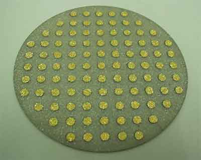 materials are extremely difficult to grow and produce, and therefore, are often not viable for manufacturing. Several research institutes have focused their efforts on bonding and fabricating mosaic single-crystal wafers. The main problem is how to align the Ori of the crystals. The size of the substrates is too small to allow the growth of polycrystals and graphite, which prevent the bonding process.
In order to mass-produce Single Crystal Diamond Wafers, a direct process is used. This process creates a diamond boule with an alternating pattern of diamond and impurity layers. This method can be applied to a wide variety of applications, including semiconductors, and can be applied to a variety of substrates. The manufacturing process of these Single Crystal Wafers allows for a high-volume production.
The large-scale production of Single Crystal Diamond Wafers has many advantages. The process involves creating semiconductor devices in the laboratory and mass producing substrates without a cleanroom. The production process is remarkably fast, which allows for large-scale semiconductor applications. Moreover, these wafers can be used in a wide range of industries. It also offers the potential to produce a high-volume substrate. The process can be applied to a wide array of industries, and the benefits are clear.
Single Crystal Diamond Wafers are made from small pieces of single crystal diamonds. They have a rough surface, but are extremely durable and can withstand extreme temperatures. The thin-slice wafers can be used in applications that require high-quality single-crystal semiconductors. Besides, they are more affordable than their large-sized counterparts. These products are particularly useful for medical equipment, as they are highly sensitive to electrostatic fields.
Single Crystal Diamonds are important for semiconductor applications. These single crystals have several advantages. They are highly stable, reliable, and can be used in a wide range of applications. The single-crystal material is a perfect match for semiconductor devices. They can be produced in a variety of semiconductor production processes. Hence, this technology is gaining popularity in the semiconductor industry. In addition to its high quality, it is also highly cost-effective.
The high quality of single crystal diamonds is an essential component of high-end semiconductors. In addition to this, they can be used in high-precision optical components as well as in photovoltaic devices. The size of the wafers must be at least 4 inches in order to make them practical. If these single crystals are used in semiconductor manufacturing, they can reduce energy consumption. Currently, they are mainly used in lasers, while they are not suitable for other applications.
The development of Single Crystal Diamond Wafers is one of the most significant advancements in semiconductor manufacturing. A single crystal diamond is a valuable component for semiconductor and optical products. It can be used in lasers, in electronics, and in optical fibers. It can also be utilized as a semiconductor. This technology allows for a wider range of applications than possible. Aside from semiconductor applications, Single Crystal Diamonds are also used for other semiconductor and electronic components.
In phase I, single crystal diamonds are grown on a ceramic substrate. The first stage of the development is the fabrication of large-scale mosaic single crystal diamond wafers. It is crucial to ensure the quality of the material and avoid the presence of other materials. While this process has many challenges, it is possible to manufacture a large-sized Single Crystal Diamond in one day. The technology is the future of the semiconductor industry and will be used in future electronic devices.
The development of SAW devices based on Single Crystal Diamond Wafers is an exciting technology. These single-crystal diamonds are available in a variety of sizes, ranging from 10x10mm to four-inch diameter. These single-crystal diamonds can be used in MEMS and tribological tests. These products are also a part of the UNCD materials, such as single-crystal diamonds and single crystals.
Is a Diamond Better Than Silicon For Computer Chips?
The use of diamonds as a replacement for silicon in computer chips is a fascinating development. Not only do diamonds handle higher voltages than silicon, but they operate with ninety percent power efficiency. Nanodiamonds, a type of diamond, can also replace vacuum tubes in high-power wireless communication systems. If you're wondering whether a diamond is better for your computer, you'll be glad to know that many other applications may also benefit from their use.
Akhan Semiconductor uses diamonds instead of silicon for computer chips
The founder of AKHAN Semiconductor, Adam Khan, has developed a cost-effective way to impose diamond wafers onto silicon. Silicon is a common material for semiconductors, but it can't withstand the extreme temperatures that diamonds can. As a result, diamond semiconductors would require less components to control the heat, and the overall footprint would be smaller.
The company's scientists use microwaves to heat a special reactor and inject methane, a gas that looks like superheated water. The diamond material is produced in sheets 1/70th the diameter of a human hair. Diamond semiconductors can be made as flexible as a human hair and would be better suited for power electronics. The technology has already received many awards and is expected to make it a viable option for low-voltage consumer electronics.
Another way diamonds can be used for computer chips is as an electrical barrier layer. Its superior thermal conductivity and high-frequency performance make it a viable alternative to silicon for many electronic devices. This technology is also significantly cheaper than other semiconductors. In the future, diamond may even replace silicon completely. And who knows? Perhaps you might be pleasantly surprised. You might be surprised at how well it works.
Earlier, this technology was considered the holy grail of electronics. However, it has become a practical alternative for silicon. It has become a viable option for both standalone semiconductor platforms and silicon supplements. This technology has the potential to change the way we use electronic devices, from cars to cell phones. And the benefits go beyond performance. Diamond semiconductors also reduce electronic waste and cut cooling costs in half.
Diamonds handle higher voltages
Diamonds are a promising material for use in computer chips because they can handle much higher voltages than silicon. This unique property of diamonds allows them to be used in high-power applications such as data-center switches. These new materials have the ability to handle higher voltages than silicon for computer chips. In addition, diamonds can handle much higher currents than silicon. However, it is not possible to produce high-voltage transistors made of diamonds at present.
Among the many properties of diamond, the ability to handle massive voltages is a huge advantage. The material can be fabricated into high-voltage semiconductors at a lower cost and requires half the material needed for silicon. Diamond semiconductors also have the lowest on-state resistance, highest saturation drift velocity, and highest breakdown voltage. They can also be up to 1,000 times thinner than silicon and be significantly smaller. Additionally, they are more energy efficient than silicon semiconductors.
However, one major limitation with diamond is its atomic size. While silicon can grow atomically-perfect monolayers on large wafers, diamond cannot. This problem has led to a number of breakthroughs in silicon semiconductor technology, including the development of microcrystalline diamond (MCD) devices and ultrananocrystalline diamond films. In silicon computer chips, the smallest atoms are just 5 nm in diameter, and the biggest difference between a silicon chip and a carbon chip is that diamonds are much more resistant to oxidation.
The latest breakthrough in diamond technology could lead to the development of better computer chips. Diamonds are better than silicon as a semiconductor, but they have limitations. Because they are thermally conductive, they can withstand higher voltages than silicon. Diamonds also handle higher powers and temperatures than silicon, reducing the need for cooling fans. In the future, computer chips could be made out of diamonds and be fabricated with no silicon at all.
Adam Khan, the founder and chief executive of Akhan Semiconductor, has made significant breakthroughs in this technology. His technology is already used in displays, chips and optics. He is a frequent speaker and has been recognized by the United States Congress. The company also has an impressive patent portfolio and a pilot facility for diamond deposition on silicon wafers. If these technologies become mainstream, the industry will benefit greatly.
Diamonds operate with over 90% increased power efficiency
A common challenge facing materials scientists is the development of efficient, compact heat sinks for semiconductor electronics. Copper and aluminum have relatively low electrical resistance, but they exhibit high thermal conductivity of around 250 W/mK and 400 W/mK, respectively. Diamonds, on the other hand, demonstrate the highest thermal conductivity of any bulk material studied. These properties make diamonds ideal heat sinks for high-power, high-frequency transistors, LEDs, and other semiconductors.
The diamond semiconductor device was fabricated by SU scientists, who discovered a new principle for its operation. The device had a dramatically increased output power and no degradation phenomenon, while exhibiting nearly identical physical properties to gallium nitride and silicon carbide. The device was able to operate with a power capability that is almost 50% higher than silicon and one-tenth the size and weight of conventional silicon-based semiconductors.
Because diamonds are so powerful and can withstand high temperatures, they have many benefits over silicon-based semiconductors. The new semiconductor technology can withstand the harsh environment of deep space and electricity grids. Further, it can withstand high voltages and can accommodate faster electrons and holes. Computer chips using diamond-based semiconductors can deliver up to a million times more electrical current than silicon-based devices.
In addition to its performance and energy-efficiency, diamond semiconductors are expected to lower the cost of electronic devices and lead to cheaper and faster cloud integration. The innovation may even change where and how we use our electronic devices. The benefits of diamond semiconductors extend beyond performance, however, and they could reduce electronic waste and cut cooling costs in half. This new technology is a game changer for all of us.
Nanodiamonds can replace vacuum tubes in high-power wireless communication
Researchers at Vanderbilt University have developed diamond versions of transistors and logical gates, two important elements in computers. In an Aug. 4 paper in Electronics Letters, the researchers describe their methods for producing nanodiamond devices. The team, which includes graduate student Nikkon Ghosh, believes that diamonds are a practical replacement for vacuum tubes in high-power wireless communication.
The manufacturing process for semiconductors involves modifications that may require changes to the packaging process. Currently, semiconductor chips are packaged in packages with inert gases or plastic to protect them from chemical degradation. Davidson and his colleagues looked into the process used to package the semiconductor chips. Currently, the seals used in military-grade circuitry are sturdy enough to hold a vacuum for centuries. By modifying the packaging process, nanodiamonds can be used as a substitute for vacuum tubes in high-power wireless communication.
However, detailed analysis of this new material is still lacking. In general, the emergence of nanodiamonds as a replacement for vacuum tubes in high-power wireless communication has been expected, but detailed analysis is needed. One of the leading rationales for using a high aspect ratio nanowire in field emission applications is based on geometry. For example, a nanodiamond emitter can be modeled as a whisker-like one-dimensional material.
The process of patterning MWCNTs can be controlled by photolithography or liquid phase electrophoretic deposition. The film thickness is controlled by the duration of the deposition and the magnitude of the applied voltage. The deposition method allows for accurate control over thickness, but sample-to-sample reproducibility is difficult. The method involves the use of common binders and is far from pure.
The process of graphitization begins with the formation of dangling bonds in the DND surface. These bonds may be saturated with species present in the annealing atmosphere. Once these dangling bonds form, they combine to form local carbon-based graphite. Further, surface graphitization begins from non-diamond carbon on the ND surface. Surface graphitization begins in the range of 700-800 degC.