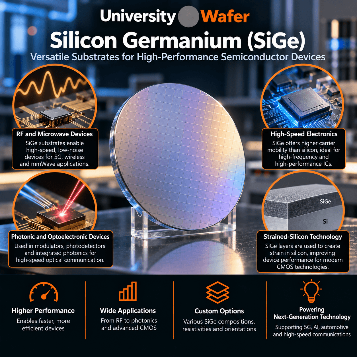
Silicon Germanium (SiGe) Wafers
Silicon Germanium (SiGe) wafers combine the proven performance of silicon with the enhanced electrical properties of germanium, making them ideal for high-speed CMOS, BiCMOS, RF devices, silicon photonics, and advanced semiconductor research. UniversityWafer supplies high-quality SiGe substrates and epitaxial wafers with customizable germanium concentrations, doping, crystal orientations, wafer diameters, and layer thicknesses to meet the demanding requirements of research laboratories, universities, and semiconductor manufacturers.
Custom Silicon Germanium (SiGe) Wafers
UniversityWafer supplies premium Silicon Germanium (SiGe) wafers and epitaxial substrates for high-speed electronics, RF integrated circuits, silicon photonics, MEMS, and advanced semiconductor research. We offer standard and custom SiGe wafers with precise germanium concentrations, epitaxial layer thicknesses, doping profiles, and crystal orientations to meet your project requirements.
Recent Research Inquiry
"We are developing high-frequency SiGe HBT devices and require 200 mm silicon germanium epitaxial wafers with approximately 30% germanium content, p-type doping, <100> orientation, and a low-defect strained SiGe layer suitable for RF characterization."
Reference #196143
Available SiGe Wafer Specifications
- 100 mm, 150 mm, 200 mm, and custom diameters
- Strained and relaxed SiGe epitaxial layers
- Custom germanium concentrations
- P-type and N-type doping options
- <100>, <110>, and <111> crystal orientations
- Prime Grade and Research Grade substrates
- Single Side Polished (SSP) and Double Side Polished (DSP)
- Custom epitaxial layer thicknesses and resistivity
Get Your Silicon Germanium (SiGe) Wafer Quote FAST! Or
Buy Online
and Start Researching Today!
What Are Silicon Germanium (SiGe) Wafers?
Silicon Germanium (SiGe) wafers are semiconductor substrates that
combine silicon with germanium to improve carrier mobility, increase switching
speeds, and enhance overall device performance. By incorporating germanium into
the silicon crystal lattice, SiGe materials provide superior electrical
characteristics while remaining compatible with conventional
silicon wafer
manufacturing processes. SiGe technology has become an important platform for
high-frequency integrated circuits, advanced CMOS devices, silicon photonics,
and next-generation semiconductor research.
Why Use SiGe Instead of Pure Silicon?
Silicon Germanium offers several advantages over traditional silicon substrates.
The addition of germanium increases carrier mobility, allowing electrons and
holes to move more efficiently through the material. This results in faster
transistor switching speeds, improved RF performance, lower operating voltages,
and reduced power consumption. Because SiGe devices can often be fabricated
using existing silicon processing equipment, manufacturers gain significant
performance improvements without completely changing their fabrication
infrastructure.
Strained and Relaxed SiGe Structures
SiGe wafers are available with both strained and
relaxed epitaxial layers. Strained SiGe creates lattice stress
that significantly improves carrier mobility, making it ideal for high-speed
CMOS transistors and RF integrated circuits. Relaxed SiGe provides a stable
platform for growing additional semiconductor layers and is widely used in
silicon photonics, heterojunction devices, and advanced electronic structures.
Germanium concentration, epitaxial thickness, doping type, and resistivity can
all be customized for specific applications.
Applications of Silicon Germanium Wafers
SiGe substrates are widely used throughout the semiconductor industry because
they combine excellent electrical performance with compatibility with silicon
fabrication technology. Common applications include:
- High-speed CMOS and BiCMOS integrated circuits
- RF and microwave communication devices
- 5G and wireless communication technology
- Silicon photonics and optical transceivers
- Heterojunction bipolar transistors (HBTs)
- MEMS and advanced sensor devices
- Infrared detectors and imaging systems
- Quantum computing and advanced semiconductor research
Custom Silicon Germanium Wafer Specifications
UniversityWafer supplies high-quality Silicon Germanium wafers with customizable
specifications to support both research and commercial production. Available
options include custom germanium concentrations, strained or relaxed epitaxial
layers, p-type and n-type doping, multiple crystal orientations, wafer
diameters from 100 mm to 300 mm, and both
single-side polished
and
double-side polished
finishes. These wafers are designed to meet the demanding requirements of
semiconductor manufacturers, research laboratories, and university engineering
programs worldwide.
Related Internal Links