
What Are Silicon Wafer Gratings?
Silicon wafer gratings are periodic structures patterned into or onto silicon substrates to control the propagation of light. Depending on their geometry, these structures can produce diffraction, coupling, reflection, filtering, or interference effects that are useful in photonics, spectroscopy, optical sensing, and integrated optical devices.
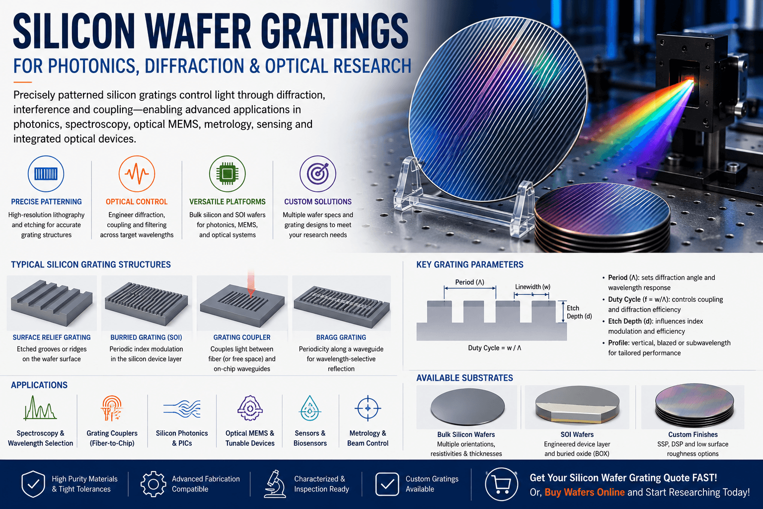
A grating typically consists of a repeating series of lines, grooves, ridges, or refractive-index variations characterized by parameters such as grating period, linewidth, duty cycle, groove depth, and profile. UniversityWafer supplies silicon wafers suitable for lithographic patterning, etching, thin-film deposition, and other processes used to develop custom grating structures.
How Diffraction Gratings Work
A diffraction grating contains a periodic structure that causes incident electromagnetic waves to interfere constructively in specific directions. For a simple grating in a uniform medium, the relationship between wavelength, grating period, incidence angle, and diffraction angle can be described by an appropriate form of the grating equation.
The exact optical response depends on more than grating period alone. Groove profile, etch depth, duty cycle, polarization, refractive indices, wavelength, angle of incidence, and the surrounding optical structure can all influence diffraction efficiency and the distribution of optical power among diffraction orders.
Why Use Silicon for Optical Gratings?
Silicon is an important material for optical gratings because it combines mature semiconductor processing with useful optical properties. Silicon can be patterned with high precision using photolithography , electron-beam lithography, and other patterning techniques, followed by controlled wet or dry etching.
Crystalline silicon has a relatively high refractive index in wavelength regions where its optical absorption is sufficiently low. This high index contrast can enable compact photonic structures, particularly when silicon is combined with a lower-index material such as silicon dioxide.
Silicon is strongly absorbing at many visible wavelengths, so it should not be described as a universally transparent optical material. Its optical suitability depends on wavelength, doping, temperature, structure, and device design. Silicon is particularly important for many near-infrared photonic applications.
Silicon-on-Insulator Gratings for Photonics
Silicon-on-insulator (SOI) wafers are widely used for integrated silicon photonics. A typical SOI substrate contains a crystalline silicon device layer separated from the silicon handle wafer by a buried silicon dioxide layer known as the buried oxide (BOX).
The refractive-index contrast between silicon and SiO₂ enables strong optical confinement in appropriately designed waveguides. Periodic structures patterned into the silicon device layer can form grating couplers, Bragg gratings, resonant structures, and other photonic components.
Silicon Grating Couplers
Silicon grating couplers are periodic structures commonly used to couple light between an integrated optical waveguide and an external optical beam or fiber. The grating provides an additional momentum component that allows light to transition between guided and radiated modes under suitable phase-matching conditions.
Coupling efficiency and bandwidth depend on factors including grating period, fill factor, etch depth, number of periods, waveguide geometry, operating wavelength, polarization, fiber angle, and surrounding refractive-index environment.
Grating couplers are widely studied for optical communications, spectroscopy, sensing, photonic integrated circuits, and wafer-scale testing of silicon photonic devices.
Bragg Gratings on Silicon
A Bragg grating introduces a periodic modulation of the effective refractive index along an optical propagation path. At wavelengths satisfying the Bragg condition, coherent reflections from successive periods can add constructively, producing wavelength-selective reflection or filtering.
Silicon Bragg gratings can be incorporated into waveguides for optical filters, wavelength-selective reflectors, resonators, sensors, and photonic integrated circuits. Their spectral response depends on parameters such as grating period, modulation strength, grating length, waveguide effective index, and fabrication tolerances.
Fabricating Gratings on Silicon Wafers
Fabrication generally begins with a clean, polished silicon or SOI substrate. A resist layer is applied and patterned using an appropriate lithography technique. The resulting resist pattern can then be transferred into the silicon or another material layer through an etching process.
Researchers developing these structures can explore wafers for microfabrication to learn more about substrate selection for lithography, thin-film deposition, etching, MEMS, photonics, and other microscale fabrication processes.
The required patterning method depends on the grating dimensions. Conventional optical lithography can be suitable for many microscale structures, while smaller-period or nanoscale gratings may require higher-resolution techniques such as electron-beam lithography or other advanced patterning methods.
Dry Etching of Silicon Grating Structures
Reactive ion etching (RIE) and related plasma processes are commonly used to transfer grating patterns into silicon. Directional plasma etching can produce controlled feature depths and relatively anisotropic profiles, which are important for many optical structures.
Etch depth, sidewall angle, sidewall roughness, linewidth, and dimensional uniformity can significantly affect optical performance. Fabrication processes therefore require appropriate control of lithography and etching parameters to reproduce the intended grating geometry.
Silicon Diffraction Gratings for Spectroscopy
Silicon diffraction gratings can be used in spectroscopic systems to separate or manipulate wavelengths through diffraction. Depending on wavelength and design, silicon can serve as the grating substrate itself or support additional reflective, dielectric, or functional coatings.
Applications can include wavelength-selective instrumentation, optical metrology, infrared spectroscopy, beam steering research, and compact optical systems. The appropriate substrate and coating depend on the spectral region and required optical efficiency.
MEMS and Tunable Optical Gratings
Microfabrication techniques can combine grating structures with MEMS to create mechanically adjustable optical components. Movement of a grating or modification of its geometry can change the optical response, enabling research into tunable filters, spectrometers, optical scanners, modulators, and sensing systems.
SOI wafers for MEMS can be particularly useful when precise structural thickness and electrical isolation are required. The silicon device layer can form mechanical or optical structures while the buried oxide can serve as an insulating, sacrificial, or etch-stop layer in suitable fabrication processes.
Wafer Surface Quality for Optical Gratings
Surface quality is an important consideration when fabricating silicon optical gratings. Excessive surface roughness, particles, scratches, lithographic defects, and etched sidewall roughness can contribute to unwanted optical scattering and reduce device performance.
Polished semiconductor substrates provide a controlled starting surface for high-resolution patterning. Depending on the application, researchers may require single-side polished (SSP), double-side polished (DSP), or application-specific surface preparation.
Chemical mechanical polishing (CMP) is one technique used in semiconductor processing to achieve highly planar surfaces where surface quality and topography control are important.
Choosing Silicon Wafers for Grating Fabrication
The appropriate silicon wafer for grating fabrication depends on both the optical design and the fabrication process. Important substrate specifications can include:
- Substrate type: bulk silicon or silicon-on-insulator (SOI)
- Wafer diameter: matched to lithography and processing equipment
- Crystal orientation: selected according to the fabrication process
- Device-layer thickness: especially important for SOI photonic structures
- Buried oxide thickness: selected according to optical and fabrication requirements
- Resistivity and doping: important when electrical functionality is integrated with the optical structure
- Surface finish: SSP, DSP, or another required preparation
- Surface roughness: important for lithography and minimizing unwanted optical scattering
- TTV, bow, and warp: relevant to lithographic focus, wafer handling, and process uniformity
Grating period, groove depth, duty cycle, linewidth, and sidewall profile are device-design parameters rather than intrinsic wafer properties. Selecting a suitable starting substrate helps provide the dimensional and surface quality needed to fabricate those structures accurately.
Applications of Silicon Wafer Gratings
Depending on grating geometry, substrate design, and operating wavelength, silicon grating structures can support research involving:
- Silicon photonic integrated circuits
- Fiber-to-chip grating couplers
- Diffraction and beam manipulation
- Optical spectroscopy
- Bragg reflectors and wavelength filters
- Optical and biochemical sensors
- MEMS-based tunable optical devices
- Infrared optical systems
- Optical metrology and calibration research
- Photonic resonators and integrated optical devices
UniversityWafer supplies silicon and SOI substrates for grating fabrication, photonics, lithography, etching, MEMS, and advanced optical research. Specify the required wafer material, diameter, orientation, thickness, device-layer thickness, oxide thickness, resistivity, and surface finish when selecting a substrate for your process.
Get Your Silicon Wafer Grating Quote FAST!
Or, Buy Wafers Online
and Start Researching Today!
Designing Silicon Gratings for Optical Applications
The performance of a silicon wafer grating depends on the geometry of the patterned structure and the optical properties of the surrounding materials. Important design parameters include grating period, duty cycle, groove depth, linewidth, sidewall profile, refractive index, operating wavelength, and polarization.
These parameters determine how incident light interacts with the periodic structure. Depending on the design, a silicon grating can function as a diffraction element, wavelength-selective reflector, fiber-to-chip coupler, resonant structure, optical sensor, or component of a silicon-on-insulator (SOI) photonic platform .
Grating Period and Diffraction Angle
The grating period is the distance over which the grating pattern repeats. For a simple diffraction grating in a uniform surrounding medium, diffraction angles are related to wavelength, incidence angle, grating period, refractive index, and diffraction order through the grating equation.
In integrated photonic structures such as grating couplers, the relationship is more complex because light begins in a guided mode with an effective refractive index. Coupler design therefore requires consideration of waveguide geometry, effective index, grating period, etch depth, cladding, wavelength, and coupling angle.
Grating Duty Cycle and Fill Factor
Duty cycle, often called fill factor in grating design, describes the fraction of each grating period occupied by one region of the periodic structure. For example, a grating containing equal-width silicon ridges and etched spaces has a nominal duty cycle of approximately 50%.
Changing the duty cycle modifies the effective optical properties of the grating and can affect coupling strength, diffraction efficiency, spectral response, and polarization sensitivity. The optimum value is therefore application-specific rather than universally 50%.
Etch Depth and Grating Performance
Grating etch depth is another important parameter, especially for gratings fabricated in silicon or the device layer of an SOI wafer. A shallow partial etch and a full etch through the silicon device layer produce different effective-index modulation and optical behavior.
For grating couplers, etch depth influences coupling strength, bandwidth, directionality, and back-reflection. For diffraction gratings, groove depth and profile can influence how optical power is distributed among diffraction orders. Accurate etch control is therefore an important part of microfabrication for optical grating structures.
Binary, Blazed and Subwavelength Gratings
Silicon can support several types of patterned grating structures. Binary gratings use repeating features with approximately two discrete height levels and are relatively straightforward to fabricate using lithography and etching.
Blazed gratings use an asymmetric groove profile designed to direct a greater fraction of optical power toward a selected diffraction order at specified wavelengths and angles. Producing an accurate blaze profile may require specialized fabrication techniques.
Subwavelength gratings contain periodic features small enough relative to the operating wavelength that only selected propagating diffraction orders exist in the relevant medium. Appropriately designed subwavelength structures can behave as engineered effective-index regions and are used in photonic couplers, filters, polarization control, and other integrated optical devices.
Silicon Grating Couplers for Fiber-to-Chip Interfaces
Grating couplers are widely used in silicon photonics to transfer optical power between an external fiber or free-space beam and an on-chip waveguide. Periodic modulation of the waveguide region provides the momentum change required to couple between guided and radiated optical modes.
Compared with edge coupling, grating couplers can enable optical access from above the wafer surface, which is useful for wafer-level testing and vertically accessible photonic circuits. However, coupling efficiency, bandwidth, polarization response, and back-reflection must be considered during device design.
SOI substrates are commonly selected for these devices because their silicon device layer and buried oxide provide strong refractive-index contrast for integrated waveguides.
Bragg Gratings and Wavelength-Selective Devices
Silicon Bragg gratings use periodic modulation along an optical waveguide to create wavelength-selective reflection. Near the Bragg condition, reflections from successive periods can interfere constructively, producing a stopband or strong reflection over a designed spectral range.
Bragg gratings can be used in optical filters, resonators, wavelength selectors, distributed reflectors, and sensing structures. Their response depends on grating period, effective refractive index, modulation strength, grating length, loss, and fabrication accuracy.
Silicon Gratings for Optical Sensing
Silicon photonic gratings can also be designed as optical sensors. Changes in temperature, strain, surrounding refractive index, or surface-bound materials can modify the effective optical properties of the grating and shift its spectral response.
These effects can be used in research involving chemical sensors, biosensors, refractive-index sensors, temperature sensors, and integrated lab-on-a-chip systems. Functional coatings or surface treatments may be added when selective interaction with a particular chemical or biological species is required.
Silicon Diffraction Gratings for Spectroscopy
A silicon diffraction grating can spatially separate wavelengths because different wavelengths satisfy the diffraction condition at different angles. This principle is fundamental to many spectroscopic instruments.
Depending on the wavelength range, the grating can consist of patterned silicon alone or incorporate reflective or dielectric coatings. Silicon is particularly relevant to infrared and microfabricated optical systems, but material absorption and coating performance must be considered for the intended spectral range.
Infrared Silicon Grating Applications
Silicon becomes substantially more transparent at wavelengths beyond its fundamental absorption edge and is widely used in portions of the near- and mid-infrared. This makes appropriately designed silicon gratings useful for infrared spectroscopy, sensing, communications, and photonic research.
Optical loss is not determined by intrinsic silicon absorption alone. Free-carrier absorption, doping concentration, surface roughness, scattering, temperature, coatings, and waveguide geometry can all influence practical device performance.
Silicon Gratings for MEMS Optical Devices
Grating structures can be integrated with SOI MEMS devices to create mechanically tunable optical components. MEMS actuation can move, rotate, stretch, or otherwise alter an optical structure, changing its diffraction or spectral behavior.
Potential research applications include tunable filters, compact spectrometers, wavelength-selective devices, optical scanners, modulators, and sensing systems. SOI is particularly useful when the device requires both accurately controlled mechanical thickness and integrated optical functionality.
Lithography for Silicon Grating Fabrication
The required lithography method depends primarily on feature size, pattern density, wafer area, and dimensional tolerances. Photolithography can efficiently pattern many micro- and submicrometer-scale structures when appropriate exposure equipment and process conditions are available.
Electron-beam lithography is commonly used for research structures requiring smaller features or flexible maskless pattern definition, although it is generally slower than wafer-scale optical lithography. Nanoimprint and other advanced pattern-transfer methods may also be appropriate for specific grating geometries and production requirements.
Fabrication Tolerances for Photonic Gratings
Photonic grating performance can be sensitive to small dimensional variations. Deviations in period, linewidth, duty cycle, etch depth, sidewall angle, or silicon device-layer thickness can shift the spectral response or change coupling and diffraction efficiency.
This sensitivity becomes especially important for narrowband devices, resonant structures, and high-index-contrast silicon photonics. Accurate lithography, etch control, wafer uniformity, and metrology are therefore important for obtaining reproducible devices across a wafer.
Surface and Sidewall Roughness
Roughness at optical interfaces can scatter light out of the intended mode. In integrated silicon photonics, etched sidewall roughness can contribute to propagation loss, while surface defects can influence both optical performance and subsequent fabrication.
Starting with a high-quality polished substrate helps provide a controlled surface for lithography. Researchers requiring information about surface preparation can explore low-surface-roughness silicon wafers .
Metrology for Silicon Grating Structures
Accurate measurement is essential for comparing a fabricated grating with its intended design. Optical microscopy and scanning electron microscopy (SEM) can be used to inspect pattern geometry, while profilometry and atomic force microscopy can provide information about feature height, etch depth, and surface topography.
Atomic force microscopy (AFM) on silicon is useful when nanoscale surface and topographic measurements are required. Optical characterization can then determine properties such as spectral response, diffraction efficiency, coupling loss, or resonance wavelength.
Reflective Coatings on Silicon Gratings
Some diffraction gratings use silicon primarily as a mechanically stable, precisely patterned substrate and rely on a deposited coating to provide the desired optical reflectivity. Metals or dielectric multilayers may be selected depending on wavelength, environmental requirements, polarization, and desired efficiency.
Coating thickness and uniformity can affect optical performance and may alter the effective groove geometry. Deposition should therefore be considered as part of the grating design rather than as an independent fabrication step.
Bulk Silicon vs. SOI for Grating Fabrication
Both bulk silicon and SOI can be useful for silicon grating fabrication, but they serve different purposes. Bulk silicon is well suited to free-space diffraction gratings, micro-optical structures, MEMS components, spectroscopy research, and experiments where a buried optical isolation layer is unnecessary.
SOI is generally preferred for many integrated silicon photonic devices because its thin crystalline silicon device layer can form waveguides and gratings while the lower-index buried oxide provides vertical optical confinement.
Choosing a Wafer for Silicon Grating Research
Researchers should choose the starting substrate according to both the optical design and the intended fabrication process. Important silicon wafer specifications for grating fabrication can include:
- Substrate: bulk silicon or SOI
- Diameter: compatible with lithography and etching equipment
- Crystal orientation: selected according to fabrication requirements
- Surface finish: SSP, DSP, or another required polish
- Surface roughness: important for high-quality optical processing
- Resistivity and doping: selected when electrical functionality or optical loss is relevant
- Device-layer thickness: critical for many SOI photonic structures
- Buried oxide thickness: selected for optical confinement and process requirements
- TTV, bow, and warp: relevant to lithography and wafer-scale uniformity
The final grating specifications—including period, duty cycle, groove depth, linewidth, blaze angle, and pattern layout—are created during microfabrication and should be designed for the target wavelength, polarization, optical mode, and application.
Silicon Grating Research Applications
Silicon and SOI substrates can support grating research for:
- Silicon photonic integrated circuits
- Fiber-to-chip optical coupling
- Bragg filters and reflectors
- Diffraction gratings and spectroscopy
- Near- and mid-infrared photonics
- Optical and biochemical sensors
- MEMS tunable optical components
- Optical metrology
- Integrated resonators and wavelength-selective devices
- Subwavelength photonic structures
UniversityWafer supplies silicon wafers and SOI substrates for photonics, diffraction-grating fabrication, lithography, MEMS, optical research, and advanced microfabrication.
Related Silicon Grating & Photonics Resources
- Silicon Wafers – Explore silicon substrates by diameter, orientation, resistivity, thickness, doping, and surface finish for grating fabrication and optical research.
- Silicon-on-Insulator (SOI) Wafers – SOI substrates for silicon photonics, waveguides, grating couplers, Bragg gratings, MEMS, and integrated optical devices.
- Microfabrication Wafers & Substrates – Learn about substrates and processes for lithography, etching, thin-film deposition, MEMS, photonics, and microscale device fabrication.
- Photolithography Process – Explore photoresist coating, exposure, development, and pattern transfer for silicon gratings and other microfabricated structures.
- SOI Wafers for MEMS – Engineered SOI substrates for optical MEMS, tunable gratings, resonators, sensors, and precision micromachining.
- Low Surface Roughness Silicon Wafers – Polished silicon substrates with controlled surface quality for photonics, lithography, optical structures, and advanced research.
- Chemical Mechanical Polishing (CMP) – Learn about semiconductor surface planarization and polishing for high-quality silicon and optical device fabrication.
- Atomic Force Microscopy (AFM) on Silicon – Nanoscale surface characterization for measuring silicon topography, roughness, and microfabricated structures.
- Silicon Wafers for Anisotropic Etching – Explore orientation-dependent silicon etching for precisely defined microstructures and specialized optical components.