
Key Takeaways
Essential Points for Silicon Wafer Optimization in MEMS
- Silicon wafers form the foundation for most MEMS (Micro-Electro-Mechanical Systems) devices due to their exceptional electrical and mechanical properties
- Ultra-thin silicon wafers (50-100µm) enable more compact and efficient MEMS designs
- Advanced dicing techniques minimize material waste and improve yield rates
- SOI (Silicon-On-Insulator) wafers provide superior electrical isolation for sensitive MEMS applications
- Proper wafer preparation techniques significantly impact MEMS device performance and reliability
- Material selection must be tailored to specific MEMS applications (sensors, actuators, optical systems)
- Implementing Design for Manufacturing (DFM) principles can increase dies per wafer by up to 180%
- Comprehensive testing strategies prevent material waste and enhance overall production efficiency
- 3D integration and wafer-level packaging dramatically improve silicon utilization
- Emerging trends include heterogeneous material integration and novel microfabrication approaches
Get Your Quote FAST! Buy Online and Start Researching Today!
Introduction to Silicon Wafers in MEMS Technology
Silicon wafers serve as the fundamental building blocks for MEMS (Micro-Electro-Mechanical Systems) devices, which combine mechanical elements, sensors, actuators, and electronics on a single substrate. The unique properties of silicon make it an ideal material for MEMS fabrication, offering excellent mechanical stability, predictable electrical characteristics, and compatibility with established semiconductor manufacturing processes. Silicon's crystalline structure provides exceptional mechanical resilience while maintaining consistent performance over millions of operation cycles, a critical requirement for reliable MEMS functionality.
At UniversityWafer, Inc., we specialize in providing high-quality silicon wafers tailored to MEMS applications. As the largest international supplier of silicon wafers to universities, industry, and government research departments, we understand the critical role that wafer selection plays in MEMS device performance. Our experience in the field allows us to offer customized solutions that meet the precise specifications required for cutting-edge MEMS development across various technological domains.
MEMS technology has changed many industries by enabling tiny sensors and actuators that can be mass-produced cheaply. From accelerometers in smartphones to pressure sensors in medical devices, MEMS components are everywhere in modern technology. How well these devices work depends a lot on how effectively silicon wafers are used in their design and manufacturing. The ability to make things super small with MEMS technology has created whole new product categories that weren't possible before.
In this guide, we'll explore ways to get the most out of silicon wafers in MEMS applications. We'll cover everything from picking the right wafer and preparing it to advanced manufacturing techniques and new trends in the field. We'll look at how choosing the right materials, smart design approaches, and better processing methods can improve device performance while making manufacturing more efficient and less expensive. Understanding these basics is important for researchers, engineers, and manufacturers who want to push the limits of what's possible with MEMS technology.
Understanding Silicon Wafer Properties for MEMS Applications
To use silicon wafers effectively in MEMS applications, you need to understand their basic properties and how these affect device performance. Silicon's special combination of mechanical, electrical, and thermal properties makes it perfect for MEMS manufacturing. Silicon's crystal structure provides a consistent and predictable foundation for creating tiny mechanical parts with great precision, which is essential for high-performance MEMS devices.
Mechanical Properties
Silicon has great mechanical stability, with a Young's modulus of about 130-180 GPa (depending on crystal orientation). This high stiffness-to-weight ratio makes silicon perfect for creating tough microstructures that can handle mechanical stress. Also, single-crystal silicon doesn't suffer from mechanical hysteresis and fatigue, so MEMS devices can keep working consistently for millions of cycles. This amazing resistance to fatigue is especially valuable in applications like resonant sensors and actuators where repeated mechanical motion is key to how the device works.
For MEMS applications that need specific mechanical characteristics, understanding silicon wafer properties in detail becomes crucial. Crystal orientation (typically <100>, <110>, or <111>) significantly affects how the material responds to etching processes and mechanical forces, directly impacting the final device performance. For instance, the <111> crystal planes etch much more slowly in anisotropic etchants like KOH, creating well-defined structures with precise geometric relationships that can be used in sensor and actuator designs.
Electrical Properties
Silicon's semiconducting nature allows for the integration of both mechanical structures and electronic components on the same substrate. The electrical resistivity of silicon wafers can be precisely controlled through doping, enabling designers to create regions with specific electrical characteristics within a single device. This capability is fundamental to creating integrated MEMS solutions where sensing, actuation, and signal processing can be combined in a single monolithic structure, reducing system complexity and improving reliability.
When preparing silicon wafers for MEMS applications, considerations such as resistivity uniformity and carrier lifetime become particularly important for devices that combine sensing elements with signal processing circuitry. The ability to create precisely defined regions with different electrical properties through techniques like ion implantation and diffusion enables sophisticated functionality within compact MEMS structures, supporting applications ranging from biomedical sensors to inertial navigation systems.
Thermal Properties
Silicon's thermal conductivity (approximately 150 W/m·K at room temperature) and coefficient of thermal expansion (2.6 × 10^-6 K^-1) make it suitable for applications involving temperature sensing or thermal actuation. These properties must be carefully considered when designing MEMS devices that will operate across varying temperature environments. The relatively high thermal conductivity allows for efficient heat dissipation in power-intensive applications, while the low thermal expansion coefficient minimizes stress and deformation in structures that experience temperature fluctuations during operation.
Key Silicon Properties for MEMS Design:
- Crystal orientation affects anisotropic etching behavior
- Doping concentration determines electrical conductivity
- Surface quality impacts bonding strength and optical properties
- Thermal characteristics influence sensor calibration and reliability
- Mechanical resilience determines long-term device stability
By understanding these material properties, MEMS designers can select the best silicon wafer specifications for their specific application requirements, maximizing device performance while minimizing material waste and production costs. The interaction between these various properties often requires careful trade-offs and optimization to achieve the desired functionality, reliability, and manufacturability in the final MEMS device. Mastering these relationships is essential for pushing the boundaries of what's possible with silicon-based MEMS technology.
Advanced Wafer Selection Strategies for MEMS Design
Selecting the right silicon wafer is a critical first step in maximizing efficiency and performance in MEMS fabrication. Different MEMS applications have unique requirements that can be addressed through strategic wafer selection. The characteristics of the starting wafer material directly influence fabrication capabilities, device performance, and manufacturing yield, making this decision a foundational element of successful MEMS development. Experienced designers carefully evaluate application requirements before specifying wafer parameters to ensure optimal results.
Wafer Diameter Considerations
While the semiconductor industry has moved toward larger wafer diameters (300mm and 450mm) for high-volume production, many MEMS applications still utilize smaller diameter wafers (100mm, 150mm, or 200mm). This is often due to:
- Lower initial tooling and mask costs for research and development
- Better compatibility with specialized MEMS equipment
- Reduced material waste for low-volume production runs
- Increased mechanical stability during processing of thick structures
- Greater flexibility for prototyping and iterative design improvements
For cutting-edge applications requiring integration with advanced CMOS processes, larger diameter wafers may be necessary. At UniversityWafer, Inc., we offer silicon wafers in various diameters to accommodate different production scales and equipment compatibility requirements. The transition between wafer sizes often represents a significant investment in equipment and process development, so this decision must be carefully evaluated based on production volume projections and technology roadmaps.
Thickness Optimization
Wafer thickness directly impacts MEMS device performance and fabrication complexity. Traditional silicon wafers typically range from 300-700μm in thickness, but many MEMS applications benefit from specialized thickness options:
- Ultra-thin wafers (25-100μm): Ideal for flexible electronics, 3D integration, and applications requiring reduced thermal resistance. These wafers enable extremely compact device packages and can facilitate novel applications where mechanical flexibility is advantageous. The reduced thermal mass also improves response time in temperature-sensitive applications.
- Standard thickness (300-500μm): Suitable for most conventional MEMS devices, offering good handling durability while maintaining compatibility with standard processing equipment. This thickness range represents a practical compromise between mechanical robustness and processing requirements.
- Thick wafers (>500μm): Beneficial for applications requiring enhanced mechanical stability or deep etching. High-aspect-ratio structures like microfluidic channels and inertial sensors often benefit from starting with thicker substrates that can accommodate deep etching processes.
Our ultra-thin silicon wafers enable the development of next-generation MEMS devices with reduced form factors and improved thermal performance. Available in thicknesses of 50μm, 75μm, and 100μm, these wafers are particularly valuable for applications in drug delivery systems and carbon nanotube growth. The handling challenges associated with ultra-thin wafers can be addressed through temporary bonding to carrier substrates during processing.
Specialized Wafer Types for MEMS
Beyond standard silicon wafers, several specialized wafer types offer enhanced performance for specific MEMS applications:
SOI (Silicon-On-Insulator) Wafers
SOI wafers consist of a thin layer of silicon separated from the bulk substrate by an insulating layer (typically silicon dioxide). This structure offers several advantages for MEMS:
- Excellent electrical isolation between components
- Simplified fabrication of suspended structures
- Reduced parasitic capacitance for improved device performance
- Better control of device layer thickness
- Enhanced protection against radiation effects in harsh environments
- Simplified release processes for movable structures
The buried oxide layer in SOI wafers serves as both an etch stop and an electrical insulator, making these wafers particularly valuable for applications requiring high precision and minimal cross-talk between components. The predefined device layer thickness eliminates variability in critical dimensions of mechanical structures, improving device consistency and performance predictability across large production volumes.
Doped Silicon Wafers
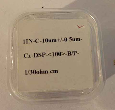
For MEMS devices that incorporate electronic components or require specific electrical characteristics, precisely doped silicon wafers are essential. The type (n-type or p-type) and concentration of dopants can be tailored to achieve desired resistivity levels, typically ranging from 0.001 to 10,000 ohm-cm. Different doping profiles can be created to optimize performance for specific applications, such as piezoresistive sensors or capacitive structures with integrated electronics.
Wafer Selection Checklist for MEMS Applications:
- Determine required diameter based on production volume and equipment compatibility
- Select appropriate thickness based on mechanical requirements and thermal considerations
- Consider specialized wafer types (SOI, doped silicon) for enhanced performance
- Evaluate surface finish requirements (polished, etched, or epitaxial)
- Specify crystal orientation based on etching behavior and mechanical properties
- Assess dopant type and concentration for electrical performance requirements
- Consider wafer bow and warp specifications for critical alignment processes
- Evaluate oxygen and carbon content requirements for specific applications
By carefully considering these factors during the wafer selection process, MEMS designers can establish a solid foundation for their devices while optimizing material usage and cost-effectiveness. Working with a knowledgeable supplier like UniversityWafer, Inc. can help navigate these options to find the ideal wafer specifications for your specific MEMS application. The right wafer choice at the beginning of the development process can significantly reduce complications in later fabrication steps and enhance overall device performance.
Optimizing Wafer Preparation for MEMS Fabrication
Proper wafer preparation is crucial for making high-quality MEMS devices that work consistently. The preparation process includes several important steps that directly affect manufacturing yield and device reliability. Even small differences in surface quality, cleanliness, or chemical composition can significantly affect later processing steps and ultimately determine whether a device works as intended. Setting up strict preparation protocols is essential for reproducible MEMS fabrication.
Crystal Growth and Wafer Manufacturing
The journey from raw silicon to MEMS-ready wafers begins with crystal growth. The two main methods are:
- Czochralski (CZ) Process: The most common method, where a seed crystal is dipped into molten silicon and slowly pulled upward while rotating, forming a large single-crystal ingot. This method is cost-effective but may introduce oxygen impurities. The controlled rotation and pull rates determine crystal diameter and quality, with modern systems capable of producing ingots up to 450mm in diameter with exceptional crystalline perfection.
- Float Zone (FZ) Process: Produces higher purity silicon by passing a molten zone through a polycrystalline silicon rod. While more expensive, FZ wafers offer superior electrical properties for sensitive MEMS applications. The absence of a crucible eliminates many sources of contamination, resulting in resistivity values that can exceed 10,000 ohm-cm with extremely low levels of carbon and oxygen impurities.
At UniversityWafer, Inc., we source silicon wafers manufactured using both methods, allowing customers to select the appropriate purity level for their specific MEMS requirements. The selection between CZ and FZ material often depends on the sensitivity of the intended application to specific impurities and the electrical isolation requirements of the final device.
Surface Preparation and Cleaning
Surface cleanliness and quality are extremely important for successful MEMS fabrication. Contaminants as small as a few nanometers can interfere with etching processes or prevent proper bonding between layers. Our comprehensive wafer preparation services include:
- RCA cleaning: A multi-step wet chemical cleaning process that removes organic contaminants, oxide layers, and ionic contamination. The standard RCA clean consists of SC-1 (NH4OH/H2O2/H2O) for removing organic contaminants, a brief HF dip for oxide removal, and SC-2 (HCl/H2O2/H2O) for removing metallic contaminants, creating an exceptionally clean surface suitable for high-precision MEMS fabrication.
- Plasma cleaning: For removing organic residues without introducing moisture. This dry cleaning method uses reactive gas species generated in a plasma to volatilize organic contaminants, leaving behind a pristine surface with controlled chemical termination that can be critical for subsequent processing steps.
- Surface activation: Preparing wafer surfaces for direct bonding applications. Techniques such as plasma activation, chemical activation, or thermal treatment can modify surface energy to promote strong bonds between silicon and various materials, enabling complex 3D structures and hermetic sealing of MEMS devices.
The chemical reactions involved in these processes must be carefully controlled. For example, the oxidation of silicon can be represented by:
SiO2 + C → Si + CO2
This reaction is critical in establishing the proper surface chemistry for subsequent processing steps. The precise control of surface termination (whether hydrogen-terminated, oxide-terminated, or otherwise functionalized) can dramatically affect adhesion, chemical reactivity, and electrical characteristics at interfaces within the MEMS structure.
Oxide and Nitride Deposition
Many MEMS devices require insulating or protective layers of silicon dioxide (SiO₂) or silicon nitride (Si₃N₄). These films serve multiple purposes:
- Electrical isolation between conductive elements
- Protection against environmental factors
- Masking layers for selective etching
- Structural components in the final device
- Stress-compensation layers to control wafer bow and mechanical behavior
- Optical components in photonic MEMS applications
The quality and uniformity of these deposited layers significantly impact device performance. Our wafer services include precise deposition of these critical films with tightly controlled thickness and composition. Techniques such as thermal oxidation, LPCVD (Low-Pressure Chemical Vapor Deposition), and PECVD (Plasma-Enhanced Chemical Vapor Deposition) are selected based on specific requirements for film density, stress, conformality, and electrical properties.
Photoresist Application and Lithography Preparation
Before photolithography can define the intricate patterns necessary for MEMS structures, wafers must be properly prepared with photoresist materials. This process includes:
- Dehydration baking to remove moisture
- Adhesion promoter application (typically HMDS)
- Precise photoresist coating with controlled thickness
- Soft baking to remove solvents and stabilize the resist
The quality of this preparation directly impacts lithography resolution and pattern transfer fidelity, which are critical for creating the fine features required in advanced MEMS devices. Modern photoresist systems can achieve feature sizes below 1 μm, but this precision requires meticulous control of the coating process, including environmental factors such as temperature, humidity, and airborne particulates.
Best Practices for MEMS Wafer Preparation:
- Maintain stringent cleanliness standards throughout the preparation process
- Characterize wafer surfaces before proceeding to subsequent fabrication steps
- Document process parameters for reproducibility and quality control
- Consider device-specific requirements when selecting cleaning and preparation methods
- Implement appropriate handling protocols to prevent contamination or damage
- Establish monitoring procedures for critical parameters like surface roughness and oxide thickness
- Develop specialized preparation sequences for unconventional materials or structures
By optimizing each step of the wafer preparation process, MEMS manufacturers can establish a solid foundation for subsequent fabrication steps, ultimately leading to higher yields and more reliable devices. Our team at UniversityWafer, Inc. provides comprehensive wafer preparation services tailored to the specific requirements of your MEMS project, ensuring that your fabrication process begins with substrates of the highest quality and consistency.
Advanced Fabrication Techniques for MEMS Devices
The fabrication of MEMS devices requires specialized techniques that enable the creation of complex three-dimensional structures with micron and sub-micron features. By employing advanced fabrication methods, engineers can maximize the utilization of silicon wafers while achieving superior device performance. These techniques have evolved significantly over the past decades, allowing for increasingly sophisticated structures with improved functionality and reliability while making more efficient use of the silicon substrate.
Bulk Micromachining Techniques
Bulk micromachining involves selectively removing portions of the silicon substrate to create three-dimensional structures. This approach is particularly valuable for devices requiring deep cavities, through-wafer holes, or suspended structures. By strategically removing material from the silicon wafer, designers can create complex mechanical elements while maintaining the excellent material properties of single-crystal silicon.
Wet Etching Processes
Wet etching uses liquid chemical etchants to remove silicon in either an isotropic (uniform in all directions) or anisotropic (direction-dependent) manner:
- Isotropic etchants like HNA (a mixture of hydrofluoric acid, nitric acid, and acetic acid) remove silicon uniformly in all directions, creating rounded features. The reaction involves the oxidation of silicon by nitric acid followed by dissolution of the oxide by hydrofluoric acid, with acetic acid serving as a buffering agent to control the reaction rate and surface quality.
- Anisotropic etchants such as KOH (potassium hydroxide) or TMAH (tetramethylammonium hydroxide) etch silicon at different rates depending on the crystal orientation, enabling the creation of precise geometric structures with well-defined angles. For example, KOH etches the {111} crystal planes approximately 100 times slower than the {100} planes, allowing for the formation of V-grooves, pyramidal pits, and other structures with precise geometric relationships.
The crystal orientation of the silicon wafer significantly impacts the etching behavior, making wafer selection a critical consideration for bulk micromachining applications. For instance, (100) oriented wafers are often preferred for creating rectangular cavities with vertical sidewalls, while (110) wafers can produce structures with vertical {111} planes that are useful for certain sensor designs.
Deep Reactive Ion Etching (DRIE)
DRIE has revolutionized MEMS fabrication by enabling the creation of high-aspect-ratio structures with nearly vertical sidewalls. The Bosch process, a common DRIE technique, alternates between:
- An etching step using SF₆ plasma
- A passivation step using C₄F₈ to protect sidewalls
This cyclic process allows for the creation of deep trenches and holes with aspect ratios exceeding 30:1, making it ideal for applications like inertial sensors, microfluidic channels, and through-silicon vias (TSVs). The characteristic "scalloping" pattern created by the alternating etch and passivation steps can be minimized through process optimization, resulting in extremely smooth sidewalls suitable for optical and fluidic applications where surface quality is critical.
Surface Micromachining Approaches
Surface micromachining builds MEMS structures by depositing and patterning thin films on the wafer surface, rather than etching into the bulk substrate. This approach is particularly suitable for creating complex, multi-layer devices with minimal silicon consumption.
The process typically involves:
- Depositing a sacrificial layer (often silicon dioxide or phosphosilicate glass)
- Patterning the sacrificial layer to define anchor points
- Depositing and patterning structural layers (typically polysilicon, silicon nitride, or metals)
- Removing the sacrificial material to release the movable structures
Surface micromachining enables the creation of intricate mechanical components like gears, springs, and cantilevers with thicknesses ranging from hundreds of nanometers to a few microns, maximizing the utilization of silicon wafer real estate. This approach is particularly valuable for creating complex mechanical systems with multiple moving parts, such as micro-mirrors for optical switching or resonant structures for RF applications.
Wafer Bonding and 3D Integration
Wafer bonding techniques enable the vertical integration of multiple wafers, creating complex 3D structures while optimizing material usage. Common bonding methods include:
- Direct (fusion) bonding: Creates a strong silicon-to-silicon bond without intermediate layers, ideal for SOI wafer fabrication. This technique relies on the formation of covalent bonds between atomically flat, hydrophilic surfaces brought into intimate contact, often followed by high-temperature annealing to strengthen the bond.
- Anodic bonding: Joins silicon to glass using electrostatic forces, commonly used for hermetic packaging. The application of high voltage across the silicon-glass interface at elevated temperatures (typically 300-500°C) causes migration of sodium ions in the glass, creating a strong electrostatic bond that is both hermetic and mechanically robust.
- Eutectic bonding: Utilizes metal alloys that form strong bonds at relatively low temperatures. Common eutectic systems include gold-silicon (Au-Si) with a eutectic temperature of 363°C and aluminum-germanium (Al-Ge) at 419°C, providing excellent mechanical strength and hermeticity.
- Adhesive bonding: Employs polymer adhesives for applications with less stringent hermeticity requirements. Polymers like BCB (benzocyclobutene), SU-8, and various epoxies can create bonds at lower temperatures with good mechanical properties, though typically with higher permeability than metal or direct bonds.
Our wafer bonding services enable the creation of complex multi-layer MEMS devices while maximizing the functional use of each silicon wafer. These techniques allow for the integration of disparate materials and processes that might not be compatible in a monolithic fabrication approach.
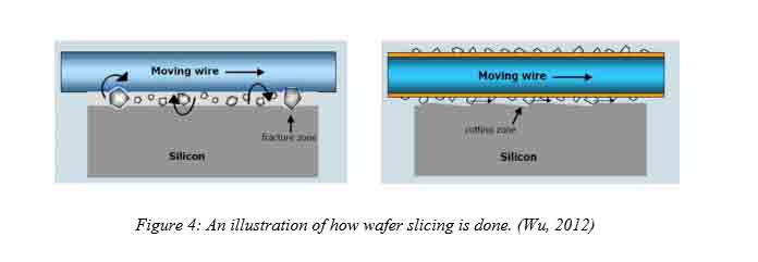
Advanced Dicing and Packaging Solutions
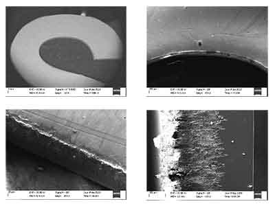
Once MEMS structures are fabricated, the wafer must be divided into individual devices through a dicing process. Traditional mechanical saw dicing can cause damage to delicate MEMS structures, leading to yield loss. Advanced dicing techniques include:
- Laser dicing: Uses focused laser energy to separate dies with minimal mechanical stress. Different laser wavelengths and pulse characteristics can be optimized for specific materials and structures, providing precise control over the dicing process while minimizing thermal damage to sensitive components.
- Plasma dicing: Employs plasma etching to create die separation trenches with high precision. This technique eliminates mechanical and thermal stress entirely, allowing for narrower dicing streets and higher die counts per wafer while preserving delicate structures that might be damaged by conventional methods.
- Stealth dicing: Creates internal modifications within the wafer using a laser, followed by mechanical separation. The laser creates a modified layer beneath the surface through multi-photon absorption, allowing for subsequent separation with minimal force and debris generation, which is particularly valuable for sensitive optical MEMS devices.
Our dicing services include these advanced techniques, allowing for optimal die separation while preserving the integrity of delicate MEMS structures. The selection of appropriate dicing technology can significantly impact both yield and device performance, particularly for fragile structures like membranes, cantilevers, and suspended masses.
Key Considerations for MEMS Fabrication Process Selection:
- Device complexity and feature requirements
- Material compatibility with subsequent processing steps
- Production volume and cost constraints
- Required dimensional accuracy and surface quality
- Integration with electronic components or other subsystems
- Environmental exposure and packaging requirements
- Thermal budget limitations for temperature-sensitive materials
- Long-term reliability and stress management considerations
By using these advanced fabrication techniques, MEMS designers can create sophisticated devices while maximizing the utilization of each silicon wafer. Our team at UniversityWafer, Inc. provides comprehensive fabrication services and expertise to help optimize your MEMS manufacturing process. Through careful selection and integration of these techniques, it's possible to achieve unprecedented levels of functionality and efficiency in silicon-based MEMS devices.
Design for Manufacturing (DFM) in MEMS
Design for Manufacturing (DFM) principles are essential for maximizing silicon wafer utilization in MEMS applications. By considering manufacturing constraints and capabilities during the design phase, engineers can significantly improve yields while reducing material waste and production costs. DFM approaches in MEMS require careful consideration of fabrication processes, material properties, and testing requirements to achieve optimal results.
Layout Optimization Strategies
Efficient wafer layout design can dramatically increase the number of functional devices per wafer. Key considerations include:
- Die size optimization: Minimizing individual die area while maintaining functionality allows for more devices per wafer. This requires careful consideration of feature scaling and the elimination of unnecessary spacing between components.
- Scribe line management: Reducing the width of dicing streets while maintaining adequate separation for cutting processes. Modern laser dicing techniques can enable narrower scribe lines compared to traditional saw dicing.
- Test structure integration: Incorporating test structures within the device area or sharing test structures between multiple dies reduces the overhead associated with process monitoring and quality control.
- Edge exclusion minimization: Optimizing the usable area near wafer edges through careful process design and equipment calibration.
Advanced layout tools and simulation software can help designers evaluate different arrangements and select the configuration that maximizes device count while maintaining manufacturability. The implementation of these optimization strategies can result in yield improvements of 50-180%, representing substantial cost savings in high-volume production.
Process Integration and Compatibility
Successful MEMS manufacturing requires careful integration of multiple fabrication processes. Design decisions made early in the development cycle can significantly impact later processing steps and overall yield. Critical considerations include:
- Thermal budget management across all processing steps
- Chemical compatibility between different materials and processes
- Stress management to prevent wafer warpage and device failure
- Contamination control throughout the fabrication sequence
- Equipment compatibility and transfer protocols between processing tools
Working with experienced suppliers like UniversityWafer, Inc. can help identify potential integration issues early in the design process, preventing costly redesigns and production delays.
Quality Control and Testing Strategies
Comprehensive quality control measures are essential for maximizing the value derived from each silicon wafer. Effective testing strategies can identify defective devices early in the production process, preventing waste of subsequent processing steps and packaging costs. Modern MEMS testing approaches combine both electrical and mechanical characterization to ensure device functionality and reliability.
Wafer-Level Testing
Testing devices while still in wafer form offers several advantages:
- Cost reduction through early identification of defective devices
- Statistical process control through comprehensive data collection
- Ability to implement corrective actions before wafer completion
- Improved traceability and yield analysis capabilities
Advanced probe stations and automated test equipment enable rapid, comprehensive testing of MEMS devices at the wafer level. This approach is particularly valuable for complex devices with multiple sensing or actuation modes that require detailed characterization.
Statistical Process Control
Implementation of robust statistical process control (SPC) methods helps maintain consistent device performance while identifying opportunities for process improvement. Key metrics typically monitored include:
- Device dimensional accuracy and uniformity
- Electrical performance parameters
- Mechanical properties such as resonant frequency and quality factor
- Environmental stability and long-term drift characteristics
The data collected through comprehensive testing programs provides valuable feedback for optimizing both device design and manufacturing processes, leading to continuous improvement in wafer utilization efficiency.
Advanced Packaging and Integration
The packaging of MEMS devices represents a critical step that can significantly impact both device performance and overall system cost. Advanced packaging technologies enable better protection of delicate MEMS structures while facilitating integration with electronic components and external systems. The selection of appropriate packaging approaches can maximize the value derived from each silicon wafer by ensuring high reliability and optimal performance in the final application.
Wafer-Level Packaging
Wafer-level packaging (WLP) techniques offer several advantages for MEMS devices:
- Reduced packaging costs through parallel processing of multiple devices
- Improved electrical performance through shorter interconnect paths
- Enhanced mechanical protection without significant size increase
- Better thermal management and environmental sealing
- Simplified assembly processes for system integration
Common WLP approaches include cap wafer bonding, thin-film encapsulation, and through-silicon via (TSV) integration. These techniques can be combined with the advanced dicing methods available through our dicing services to create highly integrated, compact device packages.
System-in-Package (SiP) Integration
System-in-Package technologies enable the integration of MEMS devices with complementary electronic components, creating complete functional systems within compact packages. This approach maximizes the value proposition of MEMS devices by providing complete solutions rather than individual components. SiP integration can include:
- ASIC integration for signal processing and conditioning
- Power management circuits for energy-efficient operation
- Wireless communication modules for IoT applications
- Additional sensors for multi-parameter measurement systems
Emerging Trends and Future Opportunities
The MEMS industry continues to evolve rapidly, driven by new applications and technological advances. Several emerging trends are creating new opportunities for maximizing silicon wafer utilization while expanding the capabilities of MEMS devices. Understanding these developments is crucial for staying competitive in this dynamic field.
Heterogeneous Integration
The integration of different materials and technologies on silicon substrates is enabling new classes of MEMS devices with enhanced functionality. Examples include:
- III-V compound semiconductors for high-frequency and optical applications
- Piezoelectric materials for improved actuation and energy harvesting
- Magnetic materials for compass and position sensing applications
- Bio-compatible materials for medical and implantable devices
These heterogeneous integration approaches require careful consideration of material compatibility, processing temperatures, and thermal expansion coefficients. Success in this area often requires close collaboration between device designers and materials suppliers to develop optimized integration processes.
Advanced Manufacturing Technologies
New manufacturing technologies are continuously expanding the possibilities for MEMS device design and fabrication:
- Atomic layer deposition (ALD) for ultra-thin, conformal coatings
- Advanced lithography techniques enabling sub-micron features
- 3D printing and additive manufacturing for rapid prototyping
- Machine learning and AI-driven process optimization
- Advanced metrology and in-situ monitoring systems
The adoption of these technologies can lead to improved device performance, reduced manufacturing costs, and enhanced reliability, all contributing to better utilization of silicon wafer resources.
Conclusion
Maximizing the use of silicon wafers in MEMS technology requires a comprehensive approach that encompasses material selection, device design, fabrication processes, and packaging strategies. Through careful application of the principles and techniques outlined in this guide, engineers and manufacturers can achieve significant improvements in both device performance and production efficiency.
Looking toward the future, emerging trends in heterogeneous integration and advanced manufacturing technologies promise to further expand the capabilities of silicon-based MEMS devices. The integration of novel materials and the adoption of advanced processing techniques will enable new classes of applications while maintaining the cost advantages that have made MEMS technology so successful.
At UniversityWafer, Inc., we remain committed to supporting the continued advancement of MEMS technology through our comprehensive silicon wafer supply and processing services. Our experience working with researchers, engineers, and manufacturers across diverse applications positions us to provide the specialized materials and expertise needed for next-generation MEMS development. Whether you require standard silicon wafers, specialized substrates like SOI wafers, or comprehensive wafer processing services, our team is ready to support your MEMS development efforts.