
SOI vs. Conventional Wafers at a Glance
- SOI wafers feature a three-layer structure (silicon/insulator/silicon) while conventional wafers have a single silicon layer
- SOI technology offers reduced power consumption (15-20% less than conventional wafers)
- SOI wafers provide complete dielectric isolation between components, eliminating latch-up
- Manufacturing methods include SIMOX, wafer bonding, and Smart-Cut technology
- SOI wafers excel in RF applications, high-performance computing, and radiation-resistant environments
- Conventional wafers remain more cost-effective for standard applications
Get Your Quote FAST! Or, Buy Online and Start Your Research Today!
Introduction to Silicon-on-Insulator (SOI) Technology
Silicon-on-Insulator (SOI) technology is one of the biggest advances in making computer chips in  recent decades. Unlike regular silicon wafers that are made of just one piece of silicon crystal, SOI wafers have three layers: a thin silicon layer on top, an insulating layer (usually silicon dioxide) in the middle, and a silicon base at the bottom. This special design changes how electronic devices work when built on these wafers.
SOI technology was created because the computer chip industry always wants better performance, lower power use, and more reliable devices in smaller packages. When regular silicon wafers started reaching their limits, SOI offered a solution to these problems.
At University Wafer, we provide many types of SOI wafers for electronics and light-based devices. These special wafers are becoming the top choice for cutting-edge computer chips where performance and efficiency matter most.
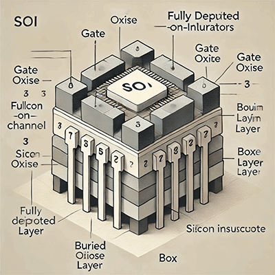
The insulating layer in SOI wafers, often called the buried oxide (BOX) layer, is what makes these wafers different from regular silicon. This layer separates the device layer from the base, which reduces unwanted electrical effects and improves device performance. Both the device layer and the BOX layer can be made in different thicknesses to fit specific needs, from nanometers to several microns.
Unlocking Photonics: SOI Wafers' Game-Changing Benefits
Silicon-on-insulator (SOI) wafers are changing how we make optical devices. These special materials help create faster, more efficient, and smaller optical devices for many industries. SOI wafers are helping researchers and engineers do new things in optical communications, sensing, and computing. Let's look at what makes SOI wafers special, how they're used, and what they might do in the future.
Key Points about Silicon-on-Insulator (SOI) Wafers
- SOI wafers have three layers: a thin silicon device layer, an insulating oxide layer, and a thick silicon handle layer
- They offer better electrical isolation and lower power consumption compared to regular silicon wafers
- SOI technology enables faster and more efficient electronic devices
- Major applications include advanced microprocessors, radio frequency devices, and photonic integrated circuits
- The global SOI wafer market is growing rapidly and expected to reach $7.86 billion by 2030
- Key manufacturing methods include SIMOX, wafer bonding, and Smart Cut processes
- SOI wafers help miniaturize electronic components and improve their performance
- Challenges include complex fabrication and higher costs compared to standard silicon wafers
- Future developments aim for ultra-thin device layers and larger wafer sizes
- SOI technology is crucial for advancing fields like 5G, artificial intelligence, and quantum computing
What Are SOI Wafers?
SOI wafers have three layers: a thin silicon layer on top, an insulating layer in the middle (usually silicon dioxide), and a thick silicon layer at the bottom. This special structure gives SOI wafers unique properties that make them great for photonic devices. The top silicon layer, which can be very thin, is where devices are made. The insulating layer, often called the buried oxide (BOX) layer, helps keep electricity where it should be. The thick silicon layer at the bottom provides support and helps manage heat.
Key Benefits of SOI Wafers in Photonics
SOI wafers have several advantages that make them really important for photonics:
1. Enhanced Performance
SOI wafers are better at controlling light because of how they're made. This means optical devices built on SOI wafers can work faster and more efficiently. They lose less light and can guide light better. SOI technology helps create fast modulators and detectors, which are important for advanced photonic circuits. Because they're good at controlling light, we can make smaller, more compact devices.
2. Lower Power Consumption
SOI wafers help optical devices use less power. The insulating layer keeps the active part of the device separate from the bottom layer, which reduces power loss. This means devices run cooler and use less energy. This is really important for big data centers and telecommunications networks, where using less energy can save a lot of money and be better for the environment.
3. Miniaturization
With SOI wafers, we can make smaller photonic components. This means we can fit more functions into a tiny space, leading to more powerful devices in smaller packages. SOI transistors, for example, can be much smaller than regular transistors but still work really well. This ability to make things smaller is crucial for developing integrated photonic circuits, where we put many optical functions on one chip.
Applications of SOI Wafers in Photonics
SOI wafers are making a big difference in various areas of photonics:
1. Telecommunications
SOI-based devices are really important for fast optical communications. They're used in fiber-optic networks and are helping to build faster, more reliable 5G systems. SOI technology in telecommunications is making it possible to send data at incredibly fast speeds, with less signal loss and better bandwidth. SOI-based components are key parts of modern optical communication systems, helping to efficiently encode, send, and receive data.
2. Data Centers
In data centers, SOI wafers are used to create efficient optical connections. These help move huge amounts of data quickly and with less energy, making data centers faster and more eco-friendly. SOI-based photonic integrated circuits (PICs) are being developed to replace traditional copper connections, offering faster data transfer and using less power.
3. Sensors and Imaging
SOI wafers are great for making sensitive optical sensors. They're used in everything from smartphone cameras to advanced medical imaging devices. SOI-based PIN diodes are especially useful for high-speed sensing. These sensors are excellent for taking pictures in low light and for spectroscopy. In medicine, SOI-based sensors are helping to develop compact, high-resolution imaging devices for non-invasive diagnostics.
4. Autonomous Vehicles
LiDAR systems, which are crucial for self-driving cars, often use SOI-based components. These help create accurate, real-time 3D maps of a car's surroundings. SOI technology allows for compact, high-performance LiDAR systems that can work reliably in different conditions. The ability to put multiple optical functions on a single SOI chip also allows for more sophisticated sensing and processing, which is crucial for the complex decision-making needed in autonomous driving.
Key Points about Silicon-on-Insulator (SOI) Wafers
- SOI wafers have three main layers: a thin silicon layer on top, an insulating layer in the middle, and a thick silicon base
- They help electronic devices work faster and use less power compared to regular silicon chips
- SOI technology is used in making advanced computer processors, sensors, and communication devices
- The market for SOI wafers is growing quickly, expected to reach $7.86 billion by 2030
- SOI wafers are made using special techniques like oxygen implantation or wafer bonding
- They're particularly useful for making tiny, powerful electronic components
- SOI technology helps reduce unwanted electrical effects in chips, making them more reliable
- Challenges include complex manufacturing processes and managing heat in dense circuits
Manufacturing SOI Wafers
Making SOI wafers requires advanced techniques. Silicon-on-Insulator (SOI) wafers feature a layered structure consisting of a thin silicon device layer, a buried oxide (BOX) insulator, and a bulk silicon substrate. This specialized design reduces parasitic capacitance and enhances semiconductor device performance, offering 30% faster switching and 80% lower power consumption compared to bulk silicon. Here are the main manufacturing methods:
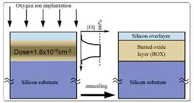
1. SIMOX (Separation by Implantation of Oxygen)
This method involves shooting oxygen ions deep into a silicon wafer. The wafer is then heated to form a buried layer of silicon dioxide. This process allows for precise control of the top silicon layer thickness and the buried oxide layer depth.
- Process Details: High-energy oxygen ions are implanted into a silicon wafer, forming a buried SiO₂ layer after high-temperature annealing at approximately 1300°C.
- Key Advantages: Provides precise control over BOX and silicon layer thickness, and creates homogeneous layers with strong thermal conductivity.
- Limitations: Can result in high defect density if annealing is insufficient, and is generally limited to thinner BOX layers compared to bonding methods.
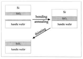
2. Wafer Bonding
Two silicon wafers are stuck together, with one having an oxide layer. The top wafer is then made thinner to create the device layer. This method starts by growing a thermal oxide on one or both of the silicon wafers. The wafers are then cleaned thoroughly and brought together under controlled conditions.
- BESOI (Bonding and Etch-back SOI): This technique bonds two oxidized silicon wafers, followed by thinning one via mechanical grinding and chemical etching. It's suitable for thick device layers (>1 μm) and offers low defect density due to post-bonding polishing, though material waste during thinning is significant.
- NanoCleave: This innovative method induces stress at the interface of silicon and silicon-germanium (SiGe) to enable precise layer separation. No chemical mechanical polishing (CMP) is required, making it scalable for 300mm wafers with 50–70% cost savings.
3. Smart Cut Technology
This advanced technique uses hydrogen ion implantation to create a thin silicon layer, which is then transferred to another wafer with an oxide layer. The process begins with hydrogen ion implantation into a silicon wafer with a thermally grown oxide layer. The implanted wafer is then bonded to a handle wafer. Heat treatment causes the hydrogen to form tiny bubbles along the implantation plane, effectively "cutting" a thin layer of silicon from the donor wafer.
- Detailed Process:
- Hydrogen ions are implanted into a donor wafer to create a stress plane
- The donor wafer is bonded to a handle wafer
- Controlled exfoliation splits the donor wafer, leaving a thin silicon layer on the handle wafer
- Unique Benefits: Allows reuse of the donor wafer, reducing costs significantly, and provides excellent thickness uniformity (±5%) without post-polishing
- Technical Considerations: Requires precise implantation dosage (5×10¹⁶–7.5×10¹⁶ ions/cm²) to minimize edge defects and prevent SOI islands (isolated silicon fragments) at wafer edges
4. ELTRAN (Epitaxial Layer Transfer)
A less common but highly effective method for specialized applications, ELTRAN creates a porous silicon layer, followed by epitaxial silicon growth and water-based splitting.
- Key Advantages: Low defect density making it suitable for high-performance RF applications
- Applications: Primarily used in advanced radio frequency circuits where signal integrity is critical
Structure and Specifications of SOI Wafers
The finished SOI wafer consists of three distinct layers:
- Device Layer (Top Silicon): 10 nm–1 μm thick, serving as the active layer for transistors
- Buried Oxide (BOX): 50 nm–1.5 μm SiO₂ layer providing electrical isolation
- Base Substrate: 100–500 μm bulk silicon providing mechanical support
Challenges and Future Innovations
Despite their performance advantages, SOI wafers face several challenges:
- Cost Factors: SOI wafers remain 10–15% more expensive than bulk silicon due to complex manufacturing processes
- Material Innovations: Research into alternative insulators such as Al₂O₃ or Ta₂O₅ layers via atomic layer deposition (ALD) offers higher thermal conductivity than traditional SiO₂
- Industry Trends: Continued evolution of Smart Cut and NanoCleave methods is driving cost reductions and performance gains for applications in 5G, IoT, and high-speed computing
Challenges and Future Developments
While SOI wafers offer many benefits, there are still challenges to overcome:
1. Cost
SOI wafers are more expensive to produce than standard silicon wafers. However, as manufacturing techniques improve and production increases, costs are expected to decrease. Researchers are looking for ways to make production more efficient and increase yield rates to make SOI technology more affordable.
2. Heat Management
The insulating layer in SOI wafers can trap heat, which can be a problem in high-power or densely packed devices. Engineers are working on innovative cooling solutions to address this issue, including advanced packaging techniques and the development of new heat-spreading materials.
3. Integration with Other Technologies
Combining SOI-based photonic components with traditional electronic circuits can be complex. Comparing SOI with conventional substrates helps in understanding these integration challenges. Researchers are developing new techniques for combining different materials and device types on a single chip.
The Future of SOI in Photonics
The future looks bright for SOI wafers in photonics, with ongoing research and development promising to unlock even more potential. Here are some exciting trends to watch:
AI Applications
Enhanced processing power for machine learning algorithms
Quantum Computing
Potential for stable qubit implementations
Photonic Integrated Circuits
Revolutionizing data transmission speeds
As these technologies develop, SOI wafers will play a crucial role in enabling faster, more efficient, and more compact photonic devices. The integration of AI accelerators on SOI platforms could lead to more powerful edge computing devices, capable of performing complex machine learning tasks with lower latency and power consumption. In quantum computing, SOI technology might provide a stable platform for implementing and controlling qubits, potentially helping to overcome some of the challenges in scaling up quantum systems. For photonic integrated circuits, ongoing advancements in SOI fabrication techniques are expected to enable even higher levels of integration, potentially leading to complete optical systems on a single chip.
Conclusion
SOI wafers are changing the world of photonics, offering better performance, lower power use, and the ability to create smaller, more efficient devices. From telecommunications to self-driving cars, SOI technology is driving innovation across many industries. The special properties of SOI wafers, including their ability to control light well and reduce unwanted effects, make them ideal for many photonic applications.
As manufacturing techniques improve and new uses are found, SOI wafers will continue to play a vital role in shaping the future of photonics and optical technologies. Ongoing research into solving current problems, such as heat management and cost reduction, promises to further improve SOI-based devices. The combination of SOI technology with other advanced materials and manufacturing techniques is opening up new possibilities for creating highly integrated, multi-functional photonic systems.
Whether you're a researcher, engineer, or just curious about cutting-edge technology, keeping an eye on SOI developments in photonics is sure to be fascinating. The benefits of SOI wafers are clear, and their impact on our technological future is only just beginning. As we move towards a more connected and data-driven world, SOI technology will likely play a crucial role in enabling the next generation of high-speed, energy-efficient optical communication systems, sensors, and computing devices. The future of photonics looks bright, and SOI wafers are at the forefront of this exciting technological revolution.
Structural Differences: SOI vs. Conventional Wafers
Physical Composition and Layer Structure
The main difference between SOI and conventional wafers is how they're built. Regular silicon wafers are made of a single piece of crystal silicon with a polished surface where devices are made. In contrast, SOI wafers have multiple layers that each serve a specific purpose.
In an SOI wafer, the top silicon layer is where active components are built. This layer can be very thin (less than 100 nm for fully depleted SOI) or several microns thick depending on what it's used for. The middle insulating layer, usually silicon dioxide (SiO₂), provides electrical isolation and is typically 0.5 to 5 μm thick. The bottom handle wafer provides physical support and makes up most of the wafer's thickness.
Electrical Characteristics and Performance
The electrical properties of SOI wafers are very different from conventional wafers because of the insulating layer. In regular wafers, transistors and other parts are directly connected to the silicon base, which can cause unwanted electrical effects and current leakage. These problems can slow down switching speed and waste power.
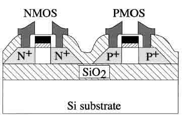
Bonded SOI wafers fix many of these issues by isolating the active device region from the base. This isolation leads to faster switching speeds, less current leakage, better control of transistor behavior, no latch-up problems in CMOS circuits, and better resistance to radiation damage.
For high-frequency applications, the reduced electrical effects of SOI wafers means better RF performance, making them perfect for fast PIN diodes and other high-frequency devices. The electrical isolation also allows components to be placed closer together without interference, saving space.
Thermal Properties and Heat Management
Heat management is one of the key differences between SOI and conventional wafers. The insulating layer in SOI wafers doesn't conduct heat as well as silicon, which can cause heat to build up in the device layer during operation. This "self-heating effect" can affect how well devices perform and how long they last in high-power applications.
Regular wafers usually handle heat better because heat can spread more easily throughout the entire silicon base. However, newer SOI designs have found ways to address heat management challenges, including optimizing device layer thickness, strategically placing thermal vias, using advanced packaging with better cooling, and spreading out heat-generating components more effectively.
For applications where heat management is critical, you need to carefully consider these thermal properties alongside performance benefits when choosing between SOI and conventional wafers.
Performance Comparison: SOI vs. Conventional Wafers
Electrical Performance and Power Efficiency
When comparing the electrical performance of SOI and conventional wafers, several key measurements show SOI's advantages. Devices built on SOI wafers typically run 20-35% faster than identical designs on conventional wafers. This improvement comes from reduced junction capacitances and lower parasitic effects.
SOI-based circuits generally use 15-20% less power than their conventional counterparts at the same performance level. This power reduction becomes even more significant at lower operating voltages, where SOI maintains better performance characteristics.
The insulating layer in SOI significantly reduces leakage currents to the substrate, which is increasingly important as devices get smaller and standby power becomes a larger part of total power consumption. SOI completely eliminates the latch-up problems in conventional CMOS circuits, improving reliability and allowing for more compact layouts.
The reduced sensitive volume in SOI devices makes them less affected by radiation-induced errors, a critical advantage for applications in harsh environments or safety-critical systems. For applications where performance per watt is the main concern, our high-performance Soitec silicon-on-insulator wafers offer significant advantages over conventional silicon.
Thermal Performance and Heat Management
The thermal characteristics of SOI wafers present both challenges and opportunities compared to conventional wafers. The buried oxide layer in SOI conducts heat about 100 times worse than silicon, which can lead to hot spots in the device layer. This self-heating effect can impact device performance and reliability, especially in high-power applications.
SOI devices typically show greater sensitivity to temperature changes, requiring more careful thermal management in system design. While sometimes challenging, the thermal isolation provided by the buried oxide can be useful in certain applications, such as thermal sensors or devices requiring thermal isolation between components.
Modern SOI designs have implemented various techniques to address thermal challenges, including strategic placement of thermal contacts, optimized device layouts to better distribute heat, advanced packaging with improved cooling, and circuit design techniques that account for self-heating effects.
When choosing between SOI and conventional wafers for high-power applications, you must carefully balance the electrical performance benefits against potential thermal management challenges.
Economic Considerations: Cost-Benefit Analysis
Manufacturing Cost Comparison
When looking at the economic aspects of SOI versus conventional wafers, manufacturing costs are an important consideration. SOI wafers typically cost 2-5 times more than conventional silicon wafers of the same size. This cost difference comes from the extra processing steps needed to create the buried oxide layer and device silicon layer.
Making devices on SOI wafers may require some changes to standard manufacturing processes, potentially adding to costs. However, these modifications are well-established in modern factories. SOI can sometimes offer yield advantages for certain device types due to reduced process variations and better isolation between components. This partially offsets the higher base wafer cost.
As SOI production volumes have increased, especially for FD-SOI technology, economies of scale have helped reduce the cost difference, though SOI remains more expensive than bulk silicon. For many applications, particularly those requiring high performance or operating in harsh environments, the premium cost of SOI wafers is justified by the performance and reliability benefits they provide.
Total System Cost and Performance Benefits
Looking beyond just the wafer cost, the total system-level economics often favor SOI for certain applications. The reduced power consumption of SOI-based circuits can mean smaller batteries, simpler cooling systems, and lower operating costs over the product lifetime.
The excellent isolation properties of SOI allow for higher component density and reduced chip area for the same functionality, potentially offsetting some of the wafer cost premium. SOI eliminates certain design challenges associated with bulk silicon, such as latch-up prevention and well spacing requirements, potentially reducing design time and complexity.
For applications where performance is the main driver, SOI's speed advantages may allow the use of lower-cost process nodes to achieve the same performance as more advanced nodes in bulk silicon.
At University Wafer, we work closely with customers to evaluate these economic trade-offs and identify the most cost-effective solution for specific application requirements, whether that involves our SOI offerings or high-purity float zone silicon wafers for more conventional applications.
Conclusion: Choosing Between SOI and Conventional Wafers
When deciding between SOI and conventional wafers for a specific application, several key factors should guide your choice. If you need maximum performance, particularly at lower operating voltages, SOI typically offers significant advantages. For battery-powered or energy-efficient applications, SOI's reduced power consumption often makes it the better choice.
Applications exposed to radiation, extreme temperatures, or other harsh conditions generally benefit from SOI's enhanced reliability. For high-frequency or sensitive analog applications, SOI's reduced parasitic capacitances and improved isolation provide substantial benefits. However, for very cost-sensitive applications where adequate performance can be achieved with conventional silicon, bulk wafers may remain the more economical choice.
Different industries have distinct priorities that influence the SOI versus conventional wafer decision. FD-SOI is increasingly favored for mobile processors and other consumer applications where the balance of performance and power efficiency is critical. The reliability advantages of SOI make it particularly valuable for safety-critical automotive systems and industrial applications operating in harsh environments.
Rather than seeing SOI and conventional wafers as competing technologies, it's better to view them as complementary solutions serving different parts of the semiconductor market. Most major semiconductor manufacturers use both SOI and conventional silicon, choosing each where most appropriate. Many complex systems use both SOI-based and conventional silicon components, taking advantage of the strengths of each technology for different functions.
As the semiconductor industry continues to evolve, both SOI and conventional silicon wafers will remain important technologies, each serving specific applications where their particular characteristics provide the best solution. At University Wafer, we provide both options and help customers select the most appropriate technology for their specific needs.
Whether your application needs the advanced performance of our Soitec Unibond SOI wafers, the specialized capabilities of our SIMOX SOI technology, or the cost-effective reliability of high-purity float zone silicon, University Wafer provides the expertise and products to support your semiconductor manufacturing needs.