
SOI vs. Conventional Wafers at a Glance
Silicon-on-Insulator (SOI) wafers use an engineered three-layer structure consisting of a thin silicon device layer, a buried insulating layer, and a silicon handle substrate. Conventional wafers are generally made from a single bulk silicon crystal.
- SOI wafers provide strong electrical isolation through the buried oxide layer.
- Reduced parasitic capacitance can support faster switching and lower-power operation.
- SOI technology can reduce substrate coupling and the risk of CMOS latch-up.
- Common manufacturing methods include SIMOX, wafer bonding, and Smart Cut layer transfer.
- SOI wafers are widely used in RF, photonics, MEMS, sensors, FD-SOI, and radiation-sensitive electronics.
- Conventional silicon wafers remain attractive for cost-sensitive and high-volume applications.
Get Your SOI Wafer Quote FAST! Or, Buy Online and Start Your Research Today!
What Is Silicon-on-Insulator Technology?
Silicon-on-Insulator technology is a semiconductor platform in which a thin crystalline silicon device layer is separated from a supporting substrate by an electrically insulating layer. This insulating layer is normally made from silicon dioxide and is called the buried oxide or BOX layer.
Unlike a conventional bulk silicon wafer, where active devices are fabricated directly within the substrate, an SOI wafer electrically isolates the active device layer from the handle wafer. This layered structure can reduce substrate leakage, parasitic capacitance, and interference between neighboring components.
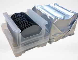
UniversityWafer supplies SOI wafers for semiconductor electronics, silicon photonics, MEMS devices, sensors, transistors, detectors, and university research.
SOI Wafer Layer Structure
A typical SOI wafer contains three functional layers:
- Silicon device layer: The upper crystalline silicon layer where transistors, waveguides, detectors, MEMS structures, and other devices are fabricated.
- Buried oxide layer: The insulating silicon dioxide layer that separates the active device region from the handle substrate.
- Handle wafer: The thicker lower substrate that provides mechanical support and determines most of the total wafer thickness.
The device-layer and BOX thicknesses can be customized for the intended application. Ultra-thin device layers may be used for fully depleted transistors, while thicker silicon layers may be preferred for MEMS, photonics, sensors, and power-device research.
Why Use SOI Wafers?
SOI wafers are selected when a device requires stronger electrical isolation, reduced substrate interaction, or precise control of the active silicon layer.
Reduced Parasitic Capacitance
The buried oxide separates the active silicon layer from the bulk substrate, reducing junction capacitance and unwanted electrical coupling. This can improve switching behavior and high-frequency performance.
Lower Leakage and Power Consumption
By limiting current paths through the substrate, SOI device structures can reduce leakage current and support energy-efficient operation. The actual improvement depends on the transistor design, process technology, operating voltage, and layer specifications.
Improved Device Isolation
The BOX layer provides dielectric isolation between the active silicon region and the handle substrate. This helps reduce substrate noise and interference between nearby devices.
Compact Device Integration
Strong isolation allows active and passive components to be placed close together while limiting unwanted interaction. This is useful in integrated electronics, RF circuits, photonic chips, and mixed-signal devices.
SOI Wafers for Silicon Photonics
SOI is one of the most widely used substrate platforms for silicon photonics. The high refractive-index contrast between silicon and silicon dioxide helps confine light within nanoscale silicon structures.
This makes it possible to fabricate compact optical waveguides, modulators, resonators, couplers, filters, and detectors on a silicon chip. The buried oxide helps isolate the optical mode from the handle substrate and reduces optical leakage.
Benefits of SOI for Photonic Devices
- Strong optical confinement in the silicon device layer
- Compact waveguide dimensions
- Integration of optical and electronic components
- Compatibility with many semiconductor fabrication processes
- Support for high-speed optical communication systems
- Scalable fabrication of photonic integrated circuits
Common SOI Photonics Applications
Optical Communications
SOI wafers are used to fabricate photonic integrated circuits for transmitting, routing, modulating, and detecting optical signals. These devices are important in fiber-optic communication networks, data centers, and high-bandwidth computing systems.
Data-Center Interconnects
Silicon photonic components can help move data between processors, memory, servers, and networking equipment using optical signals rather than only electrical connections. This can support higher bandwidth and lower interconnect power.
Optical Sensors and Imaging
SOI substrates are used in optical sensors, spectrometers, interferometers, imaging systems, and photodetectors. Researchers may also use SOI wafers for fast PIN diodes and high-speed light-detection devices.
LiDAR and Autonomous Systems
Integrated photonic components fabricated on SOI can be used in LiDAR transmitters, receivers, beam-steering systems, and optical sensing platforms. These technologies are being studied for autonomous vehicles, robotics, mapping, and industrial sensing.
Biomedical and Chemical Sensing
SOI waveguides and resonators can detect changes in refractive index near the silicon surface. This makes them useful for compact chemical sensors, biosensors, diagnostic devices, and lab-on-a-chip research.
SOI Transistors and Integrated Electronics
SOI wafers are also widely used for transistor fabrication. In a Fully Depleted SOI transistor, the silicon device layer is thin enough for the active channel to become fully depleted during operation.
This structure can improve electrostatic control, reduce leakage, and support operation at lower voltages. FD-SOI technology is used in low-power processors, RF circuits, automotive electronics, sensors, mixed-signal devices, and radiation-sensitive systems.
How Are SOI Wafers Manufactured?
SOI wafers can be produced using several manufacturing methods. The appropriate process depends on the required device-layer thickness, BOX thickness, wafer diameter, defect density, uniformity, and final application.
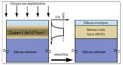
SIMOX
SIMOX stands for Separation by Implantation of Oxygen. High-energy oxygen ions are implanted below the surface of a silicon wafer. A high-temperature annealing process then forms a continuous buried silicon dioxide layer beneath the remaining silicon surface.
SIMOX can provide controlled silicon and BOX layers for semiconductor, sensor, RF, and radiation-tolerant device research.
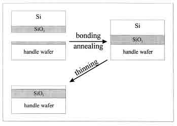
Wafer Bonding and Etch-Back
Bonded SOI is formed by joining two prepared wafers. An oxide layer is grown or deposited on one or both surfaces before bonding. One wafer is then thinned by grinding, chemical etching, polishing, or a combination of these methods.
Bonded and etch-back SOI is particularly useful when researchers require relatively thick silicon device layers for MEMS, photonics, sensors, or specialized device fabrication.
Smart Cut Layer Transfer
Smart Cut technology uses ion implantation, wafer bonding, and controlled layer separation to transfer a thin silicon layer from a donor wafer to an oxidized handle wafer.
- Hydrogen or another light ion is implanted into the donor wafer.
- The donor wafer is bonded to the prepared handle wafer.
- Thermal treatment separates the donor wafer along the implanted plane.
- The transferred silicon layer is finished to the required thickness and surface quality.
This process can produce highly uniform device layers and is widely associated with advanced engineered SOI substrates, including Soitec UNIBOND SOI wafers.
ELTRAN
Epitaxial Layer Transfer, or ELTRAN, uses a porous silicon release layer and epitaxial silicon growth. The upper silicon layer is transferred to another substrate, creating an engineered SOI structure.
ELTRAN may be used for specialized applications requiring high crystalline quality and controlled silicon layers.
Typical SOI Wafer Specifications
Researchers requesting an SOI wafer should specify the electrical, mechanical, and structural properties needed for the fabrication process.
- Wafer diameter
- Device-layer thickness
- Buried oxide thickness
- Device-layer doping type
- Device-layer resistivity
- Handle-wafer doping and resistivity
- Crystal orientation
- Total wafer thickness
- Surface finish
- Thickness uniformity
- Prime, test, or research grade
Available specifications vary by manufacturing method, wafer diameter, inventory, and quantity.
Challenges of SOI Technology
Higher Substrate Cost
SOI wafers require additional processing compared with conventional silicon wafers. Bonding, implantation, layer transfer, annealing, thinning, and polishing can increase the cost of the starting substrate.
Thermal Management
Silicon dioxide conducts heat less effectively than crystalline silicon. The buried oxide can therefore restrict heat flow from the active device layer into the handle wafer, creating a self-heating effect in some high-power devices.
Process Integration
Integrating SOI photonic, MEMS, and electronic components may require careful control of layer thickness, etching, bonding, implantation, thermal budgets, and material compatibility.
Specification Availability
Unusual combinations of device-layer thickness, BOX thickness, doping, orientation, diameter, or handle-wafer properties may require custom production or minimum quantities.
Future SOI Applications
Continued development of SOI substrates supports new research in high-speed computing, RF electronics, optical communication, advanced sensing, quantum devices, automotive systems, and heterogeneous integration.
Advanced Computing
Low-power processors, memory interfaces, accelerators, and high-bandwidth interconnects.
Quantum Devices
Engineered silicon layers for quantum sensing, cryogenic electronics, and experimental device structures.
Photonic Integration
Compact optical systems integrating waveguides, detectors, modulators, and electronic circuits.
Summary
Silicon-on-Insulator wafers combine a crystalline silicon device layer, a buried oxide insulator, and a silicon handle substrate. This structure provides strong electrical isolation and can reduce parasitic effects, leakage, substrate interference, and latch-up.
These properties make SOI valuable for FD-SOI transistors, silicon photonics, RF devices, MEMS, sensors, detectors, aerospace electronics, and advanced semiconductor research.
Conventional silicon wafers remain the practical choice for many cost-sensitive and high-volume applications. Selecting between SOI and bulk silicon requires balancing electrical performance, optical confinement, heat dissipation, fabrication compatibility, availability, and total project cost.
Structural Differences Between SOI and Conventional Silicon Wafers
Physical Composition and Layer Structure
The primary difference between Silicon-on-Insulator (SOI) wafers and conventional silicon wafers is their internal structure. A conventional wafer consists mainly of a single bulk silicon substrate, while an SOI wafer contains a thin silicon device layer, an insulating buried oxide layer, and a silicon handle wafer.
The top silicon layer of an SOI wafer is used to fabricate transistors, optical components, sensors, and other active semiconductor devices. Its thickness can range from only a few nanometers in advanced FD-SOI transistor structures to several microns for MEMS, photonics, power devices, and specialized research.
Beneath the device layer is the buried oxide (BOX) layer, typically made from silicon dioxide. This insulating layer electrically separates the active device region from the handle substrate, reducing parasitic capacitance, leakage current, and interference between nearby components.
The lower silicon handle wafer provides mechanical support and determines the overall wafer thickness. Depending on the application, the handle wafer may be standard silicon, high-resistivity silicon, heavily doped silicon, or another engineered substrate.
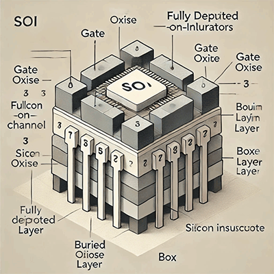
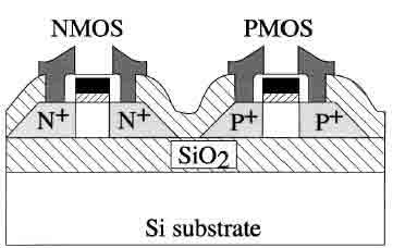
SOI Wafers vs. Conventional Silicon Wafers
| Feature | SOI Wafers | Conventional Silicon Wafers |
|---|---|---|
| Basic Structure | Silicon device layer, buried oxide, and handle wafer | Single bulk silicon substrate |
| Electrical Isolation | Excellent isolation from the BOX layer | Devices remain connected through the bulk substrate |
| Parasitic Capacitance | Reduced | Generally higher |
| Leakage Current | Lower in many device architectures | More substrate leakage paths may be present |
| Latch-Up Risk | Substantially reduced or eliminated in many SOI CMOS designs | Requires careful well spacing and isolation |
| Switching Performance | Can support faster switching through reduced parasitic effects | Depends on process node and device design |
| Power Efficiency | Well suited for low-voltage and low-power electronics | Suitable for broad general-purpose applications |
| Radiation Response | Often preferred for radiation-sensitive and aerospace devices | Larger sensitive bulk volume |
| Heat Dissipation | May require additional thermal management | Heat can spread more directly through the silicon substrate |
| Material Cost | Usually higher because of the engineered layered structure | Generally lower and broadly available |
| Typical Applications | FD-SOI, RF, MEMS, silicon photonics, imaging, sensors, and aerospace | Standard CMOS, discrete devices, power electronics, and general semiconductor fabrication |
Electrical Performance and Device Isolation
The buried oxide layer is responsible for many of the electrical advantages associated with SOI technology. In a conventional silicon wafer, transistor junctions extend into the bulk substrate, where they can interact with neighboring devices and create unwanted capacitance or current paths.
In an SOI wafer, the active silicon layer is separated from the handle wafer by an insulating oxide. This limits the amount of electrically active silicon beneath the transistor and helps reduce junction capacitance, substrate coupling, and leakage current.
These properties are particularly useful in low-power integrated circuits, high-speed transistors, radio-frequency systems, and devices that require strong electrical isolation. Bonded SOI wafers can also provide flexible device-layer and BOX thicknesses for specialized research.
Advantages of SOI Electrical Isolation
- Reduced parasitic junction capacitance
- Lower substrate leakage in many device structures
- Improved isolation between neighboring components
- Reduced risk of CMOS latch-up
- Improved signal integrity in RF and mixed-signal circuits
- Better device control at reduced operating voltages
- Smaller electrically sensitive volume in radiation environments
For high-frequency detection and switching, SOI can be used to fabricate fast PIN diodes, photodetectors, RF switches, and other devices that benefit from low capacitance and strong electrical isolation.
Power Consumption and Switching Performance
SOI-based devices can achieve strong performance at lower operating voltages because the buried oxide reduces substrate-related parasitic effects. Lower voltage operation can reduce dynamic power consumption, while improved isolation can reduce standby leakage.
The actual speed and power improvement depends on the device architecture, process technology, silicon thickness, doping concentration, BOX thickness, and circuit design. SOI should not automatically be assumed to outperform bulk silicon in every application, but it often provides an important advantage where performance per watt is a primary design goal.
Soitec UNIBOND SOI wafers are commonly used for advanced transistor, sensor, photonic, and research applications that require controlled layer thicknesses and high-quality interfaces.
Thermal Performance and Self-Heating
Thermal behavior is one of the most important tradeoffs when comparing SOI wafers with conventional silicon. Silicon dioxide has a lower thermal conductivity than crystalline silicon, so the BOX layer can restrict heat flow from the active device layer into the handle wafer.
This may produce a self-heating effect, especially in high-power or densely integrated devices. Excessive heat can shift transistor characteristics, reduce carrier mobility, and affect long-term reliability.
Conventional bulk silicon often dissipates heat more directly because the active device region is physically connected to the silicon substrate. For this reason, bulk silicon may be preferable in some high-power applications where thermal management is more important than electrical isolation.
Common SOI Thermal Management Strategies
- Optimizing the silicon device-layer thickness
- Using thermal contacts or heat-spreading structures
- Improving package-level cooling
- Separating high-power components within the layout
- Using circuit models that account for self-heating
- Selecting alternative handle substrates or engineered thermal layers
Thermal isolation can also be useful in some applications, including microheaters, thermal sensors, bolometers, and MEMS devices where heat must remain localized within a small region.
Cost and Manufacturing Considerations
Conventional silicon wafers are generally more economical because they are manufactured in high volumes using mature crystal-growth, slicing, polishing, and cleaning processes. They are widely available in many diameters, orientations, resistivities, doping types, and surface finishes.
SOI wafers require additional manufacturing steps to create the device layer and buried oxide. These steps may include ion implantation, wafer bonding, layer transfer, thinning, polishing, and high-temperature annealing. As a result, SOI substrates normally cost more than comparable bulk silicon wafers.
The higher wafer price may be justified when SOI reduces power consumption, improves device reliability, simplifies isolation, supports smaller circuit layouts, or allows a less advanced process node to meet the required performance.
Total System Cost
Engineers should evaluate more than the initial wafer price. SOI may reduce costs elsewhere in a complete system through:
- Lower power requirements
- Reduced cooling demands
- Simplified device isolation
- Reduced latch-up prevention requirements
- Improved reliability in harsh environments
- Potentially smaller chip or package dimensions
In cost-sensitive, high-volume applications where standard bulk silicon already meets the electrical and reliability requirements, conventional silicon often remains the preferred option.
When Should You Choose an SOI Wafer?
SOI wafers are often selected when electrical isolation, low parasitic capacitance, reduced leakage, compact integration, or radiation response are critical to the device design.
Applications Well Suited for SOI
- Fully depleted SOI transistors
- Low-power CMOS and embedded processors
- RF switches and high-frequency circuits
- Silicon photonic waveguides and modulators
- Photodiodes and imaging devices
- MEMS sensors and actuators
- Aerospace and radiation-tolerant electronics
- Automotive and industrial control systems
- Mixed-signal and analog circuits
- High-speed PIN diodes and detectors
When Is Conventional Silicon the Better Choice?
Conventional silicon wafers remain the best choice for many devices because they offer broad availability, mature processing, efficient heat spreading, and lower material cost.
Applications Commonly Using Bulk Silicon
- Standard CMOS integrated circuits
- Discrete transistors and diodes
- Power semiconductor devices
- Solar cells
- General microfabrication
- High-volume consumer electronics
- Research that does not require a buried oxide layer
- Applications requiring direct thermal conduction through the substrate
Researchers who need high-purity bulk silicon may consider float-zone silicon wafers, which offer high resistivity, low oxygen content, and excellent electrical properties for detectors, power devices, and scientific applications.
Common SOI Wafer Manufacturing Methods
SIMOX
SIMOX, or Separation by Implantation of Oxygen, forms the buried oxide by implanting oxygen ions beneath the silicon surface and then annealing the wafer at high temperature. The process creates a silicon device layer above a buried silicon dioxide region.
Wafer Bonding and Etch-Back
Bonded SOI is produced by joining two wafers, typically after an oxide layer has been grown on one or both surfaces. One wafer is then thinned by grinding, etching, or chemical-mechanical polishing until the required device-layer thickness is reached.
Bonded and etch-back SOI is particularly useful when a relatively thick device layer is required for MEMS, sensors, photonics, and power-device research.
Smart Cut Layer Transfer
Smart Cut technology uses ion implantation and wafer bonding to transfer a controlled silicon layer from a donor wafer to an oxidized handle wafer. After bonding, heat treatment separates the implanted layer, leaving a thin silicon film above the BOX.
This method can provide excellent device-layer uniformity and is widely associated with advanced engineered SOI substrates.
SOI Wafer Parameters to Specify
When requesting an SOI wafer quote, include the specifications that affect device performance and fabrication compatibility.
- Wafer diameter
- Device-layer thickness
- Buried oxide thickness
- Device-layer resistivity
- Device-layer doping type
- Handle-wafer resistivity
- Handle-wafer doping type
- Crystal orientation
- Surface finish
- Total wafer thickness
- Thickness uniformity
- Prime, test, or research grade
How to Choose Between SOI and Conventional Silicon
The correct wafer depends on the electrical, mechanical, optical, thermal, and economic requirements of the project.
Choose an SOI wafer when the project requires strong device isolation, reduced parasitic capacitance, low-voltage operation, compact integration, RF performance, optical confinement, or improved tolerance to radiation-induced effects.
Choose a conventional silicon substrate when cost, thermal conduction, availability, or compatibility with a standard bulk process is the main priority.
SOI and conventional silicon should not be viewed as competing solutions in every situation. They are complementary platforms designed for different semiconductor, photonic, MEMS, sensor, and research requirements.
Summary
SOI wafers provide a thin active silicon layer separated from the handle substrate by a buried oxide layer. This structure can reduce parasitic capacitance, leakage current, substrate coupling, and latch-up while supporting low-power electronics, FD-SOI transistors, RF circuits, MEMS, photonics, and radiation-sensitive devices.
Conventional silicon wafers remain the economical and widely available choice for general semiconductor fabrication, power devices, standard CMOS, and applications where direct heat conduction through the substrate is important.
UniversityWafer supplies SOI wafers, bonded SOI, SIMOX substrates, Soitec UNIBOND wafers, float-zone silicon, and conventional silicon substrates for semiconductor research and device fabrication. Selecting the appropriate structure and specifications helps ensure that the wafer matches the electrical, thermal, and manufacturing requirements of the project.