
Substrates for Flexible Organic Transistor Research
Organic field-effect transistors (OFETs) and organic thin-film transistors (OTFTs) are important building blocks for research in flexible electronics, printed sensors, wearable devices, and other large-area electronic systems. The choice of substrate affects surface roughness, dielectric properties, processing temperature, mechanical behavior, and the quality of subsequently deposited organic semiconductor layers.
UniversityWafer supplies a variety of semiconductor substrates that can be used for OFET and OTFT fabrication, process development, characterization, and flexible-device research. Depending on the device architecture, researchers may require highly doped silicon, thermally oxidized silicon, glass, quartz, or other smooth substrate materials.
Si/SiO₂ Substrates for OFET and OTFT Fabrication
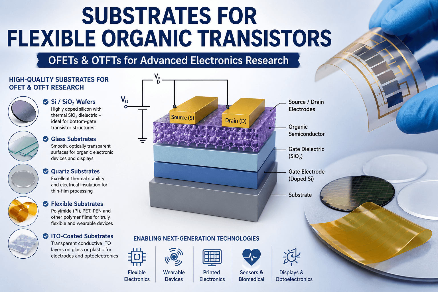
One of the most widely used laboratory platforms for studying organic transistors is a highly doped silicon wafer with a thermally grown silicon dioxide (SiO₂) layer. In a common bottom-gate OFET configuration, the conductive silicon substrate functions as the global gate electrode while the SiO₂ layer functions as the gate dielectric.
The organic semiconductor and source/drain electrodes are then formed above the dielectric according to the selected transistor architecture. This Si/SiO₂ platform is especially useful for fundamental studies because the oxide thickness and dielectric properties can be well controlled, allowing researchers to characterize parameters such as field-effect mobility, threshold voltage, on/off current ratio, and device stability.
UniversityWafer offers thermal oxide wafers with wet or dry thermally grown SiO₂ for semiconductor and transistor research. Wafer diameter, silicon conductivity, oxide thickness, surface finish, and other specifications can be selected according to the requirements of the OFET or OTFT process.
Why Highly Doped Silicon Is Used for Organic Transistors
For bottom-gate transistor test structures, highly doped silicon is often preferred because its relatively low electrical resistivity allows the substrate to serve as a convenient common gate electrode. The thermally grown SiO₂ electrically separates this gate from the organic semiconductor channel.
The dielectric layer is particularly important because its thickness, capacitance per unit area, interface chemistry, surface roughness, and defect density can influence transistor behavior. Researchers should therefore select the silicon resistivity and dielectric specifications according to the electrical requirements of their particular device rather than assuming that one wafer specification is suitable for every OFET.
Rigid Test Substrates vs. Flexible OFET Substrates
It is important to distinguish between substrates used to develop flexible transistor technology and the flexible substrate used in the final device. Conventional silicon wafers are rigid and are commonly used as controlled research platforms for developing and characterizing organic semiconductor materials. They do not provide the mechanical flexibility associated with a finished flexible transistor.
Truly flexible electronics can instead use mechanically compliant substrates such as polyimide (PI), polyethylene terephthalate (PET), polyethylene naphthalate (PEN), or sufficiently thin glass. Ultra-thin semiconductor layers can also be fabricated or transferred onto flexible carriers when higher-performance semiconductor components must be integrated into a bendable system.
Glass and Quartz Substrates for Organic Electronics
Glass-based substrates provide electrically insulating, smooth surfaces that can be useful for organic thin-film devices, sensors, displays, and transparent electronic structures. Their transparency can also be valuable when optical access through the substrate is required.
UniversityWafer supplies glass wafers and quartz substrates for thin-film deposition, materials research, sensors, and electronic device fabrication. The appropriate material should be selected according to the required surface quality, optical properties, thermal budget, dielectric behavior, and mechanical requirements.
Choosing an OFET or OTFT Substrate
There is no single ideal OFET substrate for every application. Researchers should consider the complete device architecture and fabrication process when selecting a substrate. Important parameters include:
- Surface roughness for uniform organic thin-film formation
- Gate dielectric thickness and quality for electrical performance
- Substrate conductivity when silicon is used as a gate electrode
- Thermal stability for deposition, annealing, and curing processes
- Optical transparency for optoelectronic or transparent devices
- Mechanical flexibility for bendable and wearable electronics
- Chemical compatibility with solvents, photoresists, and organic semiconductor processing
Selecting these properties carefully helps provide a reproducible platform for investigating organic semiconductor transport, dielectric interfaces, printed electrodes, and flexible transistor architectures.
Get Your Flexible Organic Transistor Substrate Quote FAST! Or, Buy Wafers Online and Start Researching Today!
Organic Field-Effect Transistor (OFET) Device Structure
An organic field-effect transistor (OFET) uses an organic semiconductor as the active channel whose conductivity is modulated by an electric field from a gate electrode. Like conventional field-effect transistors, OFETs contain a gate electrode, gate dielectric, source and drain electrodes, and a semiconductor channel.
OFETs can be fabricated using several device architectures, including bottom-gate/top-contact, bottom-gate/bottom-contact, top-gate/top-contact, and top-gate/bottom-contact structures. The optimum architecture depends on the organic semiconductor, electrode materials, dielectric, fabrication method, and intended application.
For laboratory research, highly doped silicon wafers are frequently used in bottom-gate structures. The conductive silicon can function as the gate electrode while an insulating SiO₂ layer separates the gate from the organic semiconductor channel.
Gate Dielectrics for OFET and OTFT Research
The gate dielectric is a critical component of an organic transistor because it electrically isolates the gate while capacitively coupling the gate voltage to the semiconductor channel. Common dielectric materials used in organic transistor research include silicon dioxide (SiO₂), silicon nitride (Si₃N₄), aluminum oxide (Al₂O₃), and various polymer dielectrics.
UniversityWafer supplies thermal oxide silicon wafers for OFET and OTFT research. Thermally grown SiO₂ is widely used because its thickness can be precisely controlled and it forms a high-quality insulating layer on crystalline silicon.
Dielectric thickness and relative permittivity determine the gate capacitance per unit area, which influences the charge density induced in the transistor channel at a given gate voltage. Surface chemistry, roughness, trapped charge, and interfacial defects can also affect threshold voltage, hysteresis, charge transport, and operational stability.
Why Surface Quality Matters in Organic Transistors
The interface between the organic semiconductor and the gate dielectric plays an important role in OFET performance. Because charge transport occurs close to this interface in many OFET architectures, substrate and dielectric surface properties can strongly influence semiconductor morphology and electrical behavior.
Smooth, clean substrates can promote more reproducible organic thin-film formation. Depending on the semiconductor and process, researchers may also modify the dielectric surface using self-assembled monolayers or other surface treatments to adjust surface energy and semiconductor organization.
For experiments requiring high-quality polished surfaces, researchers can select semiconductor wafers and substrates with controlled surface finish, thickness, resistivity, and dielectric specifications.
Flexible Substrates for Organic Thin-Film Transistors
One advantage of organic semiconductor technology is its compatibility with mechanically flexible substrates and relatively low-temperature fabrication processes. Flexible OTFT and OFET substrates can include polyethylene terephthalate (PET), polyethylene naphthalate (PEN), polyimide (PI), and other polymer films.
The substrate must be selected according to more than flexibility alone. Important considerations include dimensional stability, surface roughness, solvent resistance, moisture and oxygen barrier properties, thermal budget, coefficient of thermal expansion, and compatibility with deposition and patterning processes.
Learn more about substrates for flexible electronics and the role of polymer films, thin glass, ultra-thin silicon, and carrier wafers in bendable and conformal electronic systems.
ITO-Coated Substrates for Flexible and Transparent Electronics
Some organic electronic devices require an electrode that combines electrical conductivity with optical transparency. In these applications, indium tin oxide (ITO) can be deposited on glass or polymer films to create a transparent conductive electrode.
UniversityWafer offers ITO-coated glass and flexible ITO substrates , including ITO-coated PET and PEN options for research involving flexible electronics, transparent electrodes, organic devices, sensors, and optoelectronics.
Organic Semiconductor Deposition and Printing
Depending on the organic semiconductor, OFET and OTFT active layers can be formed using solution-based or vacuum-based techniques. Examples include spin coating, inkjet printing, blade coating, slot-die coating, and vacuum thermal evaporation.
Solution processing is particularly attractive for printed electronics because compatible semiconductor, dielectric, and conductive inks can potentially be patterned over large areas using additive manufacturing techniques. Vacuum deposition remains important for organic materials that are more effectively deposited as controlled thin films from the vapor phase.
The appropriate deposition process depends on semiconductor solubility, desired film thickness, molecular organization, substrate surface properties, processing temperature, and device architecture.
Source and Drain Electrodes in OFETs
The source and drain electrodes inject and collect charge carriers from the organic semiconductor channel. Metals such as gold are widely used in research devices, while silver, conductive polymers, carbon-based materials, and other electrode systems can also be used depending on the semiconductor and fabrication process.
Electrode work function, interface chemistry, contact geometry, and semiconductor energy levels influence charge injection and contact resistance. Poor electrical contacts can limit measured transistor performance even when the organic semiconductor itself has favorable charge-transport properties.
Applications of Flexible Organic Transistors
Flexible organic transistors are actively investigated for electronic systems where low weight, large-area fabrication, or mechanical compliance is valuable. Potential and demonstrated research applications include:
- Flexible and conformable sensor arrays
- Wearable electronic devices
- Electronic skin and pressure sensors
- Flexible and printed circuits
- Biomedical and biosensing devices
- Flexible display backplanes
- Organic photodetectors and optoelectronic systems
- Large-area printed electronics
- Low-voltage organic transistor research
Researchers can also explore UniversityWafer's organic transistor substrates for information about highly doped Si/SiO₂ wafers, dielectric layers, diced silicon chips, and other substrate configurations used for OFET and OTFT development.
Selecting Substrates for Flexible Organic Transistors
Substrate selection should be based on the complete device structure and fabrication process. A rigid, highly doped Si/SiO₂ substrate is often an excellent choice for controlled electrical characterization and fundamental organic semiconductor research, while PET, PEN, polyimide, or other flexible materials are more appropriate when mechanical bending is an essential property of the final device.
Researchers should specify requirements such as substrate material, dimensions, thickness, surface finish, silicon resistivity, dielectric material and thickness, transparency, and thermal-processing limits when selecting OFET and OTFT substrates.
Related Flexible Electronics & Organic Transistor Resources
- Organic Transistor (OFET) Substrates
- Substrates for Flexible Electronics
- Thermal Oxide (SiO₂) Silicon Wafers
- Silicon Wafers for Semiconductor Research
- ITO-Coated Glass & Flexible Substrates
- Glass Wafers for Thin-Film Devices
- Quartz Substrates for Electronics Research
- Semiconductor Wafers & Substrates