
Key Takeaways
- Ultra-thin silicon wafers range from 5μm to 100μm in thickness, significantly thinner than standard wafers
- Applications include flexible electronics, solar cells, lab-on-a-chip devices, and MEMS technology
- Manufacturing challenges include maintaining structural integrity during processing
- Key properties include mirror finish, good surface flatness, and low surface roughness (1-2nm)
- Thinning technologies include mechanical grinding, chemical etching, and plasma processing
Get Your Quote FAST! Buy Online and Start Researching Today!
Introduction to Ultra-Thin Silicon Wafer Technology
Silicon wafers are the foundation of modern electronics, but ultra-thin silicon wafers take this technology to new levels. These substrates, with thicknesses between 5 and 100 microns (compared to standard wafers at 500-775 microns), are changing electronics by enabling more compact, flexible, and efficient devices. For comparison, ultra-thin silicon wafers can be thinner than a human hair, which is typically 70-100 microns thick. This thinness is a major engineering achievement, allowing for new shapes and performance in semiconductor applications.
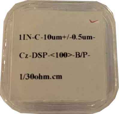
The demand for ultra-thin silicon wafers has grown as industries try to create smaller devices that work better. These wafers have great features including true mirror finish double-side polishing (DSP), excellent surface flatness, and very low surface roughness of about 1-2nm. The careful engineering that goes into making these wafers allows for better device integration and performance, making them essential in advanced electronic applications where space and heat management matter.
While standard 300mm silicon wafers remain the backbone of computer chip manufacturing, ultra-thin versions create new possibilities in special applications where flexibility, heat removal, and integration are important. The development of silicon wafer technology has been driven by the constant push for smaller and better-performing semiconductor devices. This progress represents a big advance in materials science, allowing for new devices that weren't possible with normal wafer thicknesses, like flexible displays, advanced sensors, and new medical implants.
Manufacturing Process of Ultra-Thin Silicon Wafers
Making ultra-thin silicon wafers involves complex manufacturing processes that need precise engineering and strict quality control. It starts with very pure silicon ingots, usually made using the Czochralski (CZ) method, which are then processed through many stages to reach the desired thinness while staying strong. Each step must be carefully controlled to make sure the final wafers meet the exact requirements for advanced electronic applications. Even small changes in the process can result in wafers that don't meet quality standards.
Initial Wafer Production
The manufacturing process begins with normal thickness wafers, usually 775 micrometers for 300mm wafers. These wafers are made from silicon ingots grown to have specific resistivity values (usually 1-5 ohm-cm) and crystal orientation accuracy (typically within ±2 degrees). The initial wafers are cut using diamond wire saws, then their edges are rounded, and they're lapped and polished to get a mirror-like surface. This first processing creates the foundation for later thinning operations and must meet strict quality requirements to ensure the final ultra-thin wafers will have the right electrical and mechanical properties for their intended uses.
Thinning Technologies
Several advanced technologies are used to reduce standard wafers to ultra-thin dimensions:
- Mechanical Grinding and Polishing: This traditional method uses finer and finer abrasives to thin the wafer while keeping good surface quality. It's hard to get uniform thickness below 50 microns without causing stress or damage. Advanced grinding systems use precise force control and special abrasives to minimize damage while removing material quickly.
- Chemical Etching: Wet chemical processes using solutions like potassium hydroxide (KOH) or tetramethylammonium hydroxide (TMAH) can selectively remove silicon with high precision. This helps achieve even thinning while minimizing mechanical stress. The etching process can be controlled through temperature, concentration, and timing to reach specific thickness targets with good uniformity across the wafer.
- Plasma Processing: Advanced plasma-based thinning techniques offer excellent control for making ultra-thin wafers with minimal surface damage and good uniformity. These processes use reactive ion species to remove silicon atoms from the surface through chemical and physical mechanisms, resulting in very smooth surfaces with minimal subsurface damage.
- Temporary Bonding and Debonding: To prevent warping or breakage during processing, ultra-thin wafers are often temporarily bonded to carrier wafers, processed, and then carefully separated. This provides mechanical support throughout the thinning and device fabrication processes, allowing the handling of extremely thin substrates that would otherwise be too fragile for normal processing equipment.
The challenge in making these wafers is balancing thinness with strength. As wafers get thinner, they become more fragile and likely to warp, requiring special handling equipment and environments. At UniversityWafer, manufacturing partners use modern facilities with controlled environments to ensure the highest quality standards for ultra-thin silicon wafers. These facilities maintain exact temperature, humidity, and particle control to prevent contamination and environmental factors that could hurt wafer quality during the complex manufacturing process.
Key Properties and Characteristics
Ultra-thin silicon wafers have unique properties that make them different from standard thickness wafers, making them perfect for specialized applications in advanced electronics and research. Understanding these characteristics is important for researchers and engineers working with these materials. The combination of reduced thickness with silicon's semiconductor properties creates substrates with special mechanical, thermal, and electrical behaviors that can be used for new device designs and applications not possible with normal wafers.
Surface Quality and Finish
One of the most important characteristics of ultra-thin silicon wafers is their excellent surface quality. These ultra-thin wafers feature:
- True Mirror Finish Double-Side Polishing (DSP): This provides an optically smooth surface on both sides of the wafer, essential for applications requiring high-quality interfaces or optical properties. The mirror finish is achieved through precise chemical-mechanical polishing processes that remove surface irregularities down to the atomic level, resulting in surfaces with reflectivity approaching that of optical mirrors.
- Low Surface Roughness: Typically measuring 1-2 nanometers, this extremely smooth surface is crucial for consistent device performance and reliable bonding processes. Such minimal roughness ensures optimal contact between the wafer and subsequent layers in device fabrication, minimizing interface defects that could compromise electrical performance or mechanical integrity.
- Excellent Surface Flatness: Despite their thinness, these wafers maintain remarkable flatness, which is essential for photolithography and other precision manufacturing processes. Advanced processing techniques enable total thickness variation (TTV) values as low as 1-2 microns across 300mm wafers, ensuring uniform device characteristics across the entire substrate.
Mechanical Properties
The mechanical behavior of ultra-thin silicon wafers differs significantly from standard wafers:
Ultra-thin silicon wafers can bend without breaking, unlike rigid standard wafers. Wafers thinner than 50 microns can noticeably bend without cracking. This flexibility allows them to be used in curved or conformable electronics that would be impossible with normal rigid substrates, opening new possibilities in wearable technology and biomedical devices.
The minimal thickness results in lower thermal mass, allowing for faster heating and cooling cycles, which can be helpful in certain processing steps. This enables faster thermal processing, reduced energy use, and better temperature uniformity during manufacturing processes like rapid thermal annealing.
These wafers are more sensitive to thermal and mechanical stresses, requiring careful handling and specialized processing equipment. The reduced thickness amplifies the effects of stress gradients, making stress management a critical consideration in both manufacturing and application design to prevent warping or fracture.
Electrical and Optical Properties
The reduced thickness affects several key electrical and optical characteristics:
The reduced thickness minimizes thermal resistance, allowing for better heat dissipation in high-power applications. This is particularly valuable in power electronics and high-performance computing applications where thermal management limits device performance and reliability.
Thinner substrates can reduce parasitic capacitance in certain device designs, potentially improving high-frequency performance. This enables faster switching speeds and lower power consumption in radio frequency (RF) and high-speed digital applications, contributing to overall system efficiency.
As silicon wafers become extremely thin (below 20 microns), they begin to show measurable transparency to certain wavelengths of infrared light. This can be used in specialized optoelectronic applications, sensors, and imaging devices that need both electronic functionality and specific optical properties.
Ultra-thin silicon wafers can be customized with various specifications, including different crystal orientations, dopant types (p-type or n-type), and resistivity ranges to meet specific research and manufacturing requirements. Additionally, specialized coatings like PVD (Physical Vapor Deposition) can be applied for enhanced surface properties or functionality. These customization options allow researchers and manufacturers to optimize the substrate properties for specific applications, further expanding the versatility and utility of ultra-thin silicon technology across diverse fields.
Applications in Modern Electronics
Ultra-thin silicon wafers are driving innovation across multiple industries, enabling new form factors and enhanced functionality in electronic devices. Their unique properties make them ideal for applications where standard thickness wafers would be impractical or limiting. The combination of silicon's excellent semiconductor properties with the mechanical and thermal advantages of ultra-thin substrates has created entirely new design possibilities for device engineers and researchers working at the cutting edge of electronics technology.
3D Integration and Stacked ICs
Ultra-thin silicon wafers are changing three-dimensional integrated circuit design. By stacking multiple thin layers of silicon containing different circuit elements, manufacturers can:
- Create more compact devices with higher component density, enabling unprecedented levels of functionality in smaller form factors that meet the demands of portable and wearable electronics
- Reduce signal propagation distances between components, resulting in faster operation and lower power consumption through minimized interconnect resistance and capacitance
- Improve power efficiency by minimizing interconnect lengths, addressing one of the most significant challenges in modern high-performance computing systems
- Enable heterogeneous integration of different technologies in a single package, combining memory, logic, analog, and sensor components in optimized three-dimensional arrangements
These 3D integrated circuits are finding applications in high-performance computing, memory modules, and advanced mobile processors. The reduced thickness of each layer allows for more efficient through-silicon vias (TSVs), which are vertical electrical connections passing completely through the silicon wafer. These TSVs enable high-bandwidth, low-latency communication between stacked layers, overcoming the interconnect bottlenecks that limit conventional two-dimensional circuit designs.
Flexible and Wearable Electronics
When thinned below approximately 50 microns, silicon wafers gain a degree of mechanical flexibility that enables new applications:
Flexible display backplanes for curved or bendable screens can conform to non-planar surfaces or fold for compact storage while maintaining the high performance of silicon-based transistors. Conformable sensor arrays can adapt to non-flat surfaces, enabling new form factors for environmental monitoring, structural health assessment, and human-machine interfaces.
Wearable health monitoring devices can comfortably follow body contours, providing continuous biometric data collection without the bulk and rigidity of conventional electronics. Implantable medical devices can minimize tissue stress, improving biocompatibility and patient comfort while using silicon's excellent electronic properties and established biocompatibility.
This flexibility, combined with silicon's excellent electronic properties, offers advantages over organic semiconductor alternatives in terms of performance and reliability. UniversityWafer provides ultra-thin silicon substrates to researchers developing next-generation flexible electronics. These substrates offer the performance advantages of single-crystal silicon while enabling conformability to curved surfaces, bridging the gap between conventional rigid electronics and fully flexible organic semiconductor technologies.
MEMS and Sensors
Micro-Electro-Mechanical Systems (MEMS) benefit significantly from ultra-thin silicon technology:
Enhanced sensitivity in pressure sensors and accelerometers due to the reduced mechanical stiffness of thinner structures, enabling detection of smaller physical stimuli with greater precision. Improved response time in thermal sensors due to reduced thermal mass, allowing faster detection of temperature changes and improved temporal resolution in thermal imaging applications.
More efficient electromechanical coupling in resonant structures, resulting in higher quality factors and improved frequency stability in oscillators and timing references. Reduced power consumption in portable sensor applications through minimized actuation energy requirements and improved transduction efficiency.
The precise mechanical properties of single-crystal silicon make it an ideal material for MEMS devices, and the reduced thickness enables new design possibilities while improving performance parameters. The combination of silicon's excellent mechanical stability, predictable elastic properties, and the dimensional advantages of ultra-thin substrates has enabled significant advances in sensor technology for applications ranging from consumer electronics to industrial monitoring and automotive safety systems.
Solar Cells and Photovoltaics
Ultra-thin silicon wafers are transforming photovoltaic technology by:
Reducing material costs through minimized silicon usage, addressing one of the major cost components in traditional photovoltaic manufacturing while maintaining excellent energy conversion efficiency. Improving flexibility for curved or non-planar solar installations, enabling integration into building materials, vehicle surfaces, and portable electronics where conventional rigid panels would be impractical.
Enhancing light trapping through specialized surface texturing techniques that become more effective in ultra-thin structures, improving photon absorption and overall energy conversion efficiency. Enabling higher efficiency in certain cell architectures by minimizing bulk recombination losses and improving carrier collection probability, particularly in advanced heterojunction designs.
These advantages make ultra-thin silicon an attractive option for both traditional solar panels and emerging applications like building-integrated photovoltaics and portable power solutions. The reduced weight of ultra-thin silicon solar cells also expands their potential applications in aerospace, portable electronics, and remote power systems where minimizing mass is a critical design consideration.
Lab-on-a-Chip and Microfluidics
The biomedical field has embraced ultra-thin silicon technology for creating sophisticated diagnostic platforms:
Integrated microfluidic channels with electronic sensing components enable comprehensive sample processing, analysis, and detection on a single compact substrate with minimal sample volume requirements. Miniaturized analytical systems for point-of-care diagnostics combine multiple laboratory functions in portable, low-cost devices accessible in resource-limited settings.
Implantable biosensors with minimal invasiveness leverage silicon's biocompatibility and excellent electronic properties for continuous monitoring of physiological parameters. High-throughput screening platforms for drug discovery enable parallel testing of multiple compounds with integrated sensing and analysis capabilities.
The combination of silicon's biocompatibility, excellent electrical properties, and the dimensional advantages of ultra-thin substrates makes these wafers ideal for advanced biomedical applications. The precise microfabrication capabilities developed for semiconductor manufacturing can be applied to create intricate microfluidic structures with integrated electronic functionality, enabling complex biological and chemical analysis in compact, portable formats.
Comparison with Alternative Substrate Materials
While ultra-thin silicon wafers offer exceptional properties for many applications, various alternative substrate materials are also used in specialized contexts. Understanding the comparative advantages and limitations helps researchers and engineers select the optimal material for their specific requirements. Each substrate material presents a unique combination of electrical, mechanical, thermal, and optical properties that make it suitable for particular applications while potentially limiting its utility in others.
Silicon vs. III-V Compound Semiconductors
Indium Gallium Arsenide (InGaAs) and other III-V compounds offer distinct advantages in certain applications:
- Electron Mobility: III-V materials typically provide higher electron mobility than silicon, enabling faster device operation. For instance, InGaAs can offer electron mobility values exceeding 10,000 cm²/V·s compared to silicon's typical 1,400 cm²/V·s, making III-V compounds particularly advantageous for high-frequency applications like wireless communication systems.
- Direct Bandgap: Unlike silicon's indirect bandgap, many III-V compounds have direct bandgaps, making them more efficient for optoelectronic applications. This property enables efficient light emission and absorption, critical for applications like lasers, LEDs, and high-efficiency photovoltaics where silicon's indirect bandgap limits performance.
- Cost and Processing: Silicon remains significantly more cost-effective and benefits from decades of established processing techniques. The mature manufacturing infrastructure for silicon processing allows for higher yields, larger wafer sizes, and more consistent quality compared to III-V materials, which typically require more specialized and expensive processing equipment.
- Integration Challenges: Combining III-V materials with silicon circuitry presents technical challenges that ultra-thin silicon can sometimes avoid. These challenges include lattice mismatch, thermal expansion coefficient differences, and contamination concerns that complicate heterogeneous integration efforts.
For applications requiring both high-speed operation and cost-effectiveness, heterogeneous integration of ultra-thin silicon with III-V materials represents a promising approach. This strategy leverages the complementary strengths of both material systems, combining silicon's mature processing technology and excellent cost structure with the superior electronic and optoelectronic properties of III-V compounds.
Silicon vs. Sapphire Substrates
Sapphire wafers offer unique properties that complement silicon in specialized applications:
Sapphire is transparent across a wide spectrum, making it ideal for optical applications. Its transparency extends from ultraviolet through visible and into the mid-infrared range (approximately 0.2-5.5 μm), enabling applications in optical sensors, display substrates, and specialized imaging systems where silicon's opacity would be limiting.
As an insulator, sapphire eliminates parasitic capacitance issues present in semiconducting substrates. This makes it particularly valuable for radio frequency (RF) applications where substrate losses can significantly impact device performance, providing better isolation between components and reduced signal loss.
Sapphire maintains its properties at higher temperatures than silicon. With a melting point of approximately 2,030°C compared to silicon's 1,414°C, sapphire offers exceptional stability in high-temperature environments, making it suitable for devices operating in extreme conditions like aerospace applications or high-temperature sensors.
Silicon remains more cost-effective for most applications, especially in larger diameters. Sapphire wafers typically cost 5-10 times more than comparable silicon wafers, limiting their use to applications where their unique properties justify the additional expense.
In applications like RF devices and specialized sensors, silicon-on-sapphire (SOS) technology combines the advantages of both materials. This approach integrates a thin layer of single-crystal silicon on a sapphire substrate, providing the electronic functionality of silicon with the insulating and thermal properties of sapphire for specialized high-performance applications.
Silicon vs. Silicon Carbide
Silicon Carbide (SiC) excels in high-power and high-temperature applications:
SiC's wider bandgap enables operation at higher voltages and temperatures. With a bandgap of approximately 3.2 eV for 4H-SiC compared to silicon's 1.1 eV, silicon carbide devices can withstand electric fields roughly ten times higher than silicon devices, enabling more compact high-voltage components with reduced cooling requirements.
SiC offers superior thermal conductivity, beneficial for high-power devices. With values typically around 370-490 W/m·K compared to silicon's 130-150 W/m·K, silicon carbide dissipates heat more efficiently, allowing for higher power density and improved reliability in power electronic applications.
Silicon processing is more mature and less expensive than SiC. The challenging material properties of silicon carbide, including its extreme hardness and chemical stability, make wafer production, polishing, and device fabrication more difficult and costly, limiting its adoption to applications where its superior properties justify the additional expense.
SiC is harder and more difficult to process into ultra-thin substrates. With a Mohs hardness of approximately 9.5 compared to silicon's 7, silicon carbide presents significant challenges for thinning processes, making ultra-thin SiC wafers more expensive and less readily available than their silicon counterparts.
For applications operating under extreme conditions, SiC may be preferable, while ultra-thin silicon offers advantages in cost-sensitive applications with moderate operating conditions. The selection between these materials often involves balancing performance requirements against cost constraints, with silicon carbide typically reserved for applications where its superior electrical and thermal properties provide essential performance advantages that justify its higher cost.
Silicon vs. Flexible Organic Substrates
For truly flexible electronics, organic substrates compete with ultra-thin silicon:
Organic substrates can achieve greater flexibility than even the thinnest silicon wafers. Materials like polyimide or PET can be manufactured with thicknesses below 10 microns and bend radii of a few millimeters without damage, enabling applications in rollable displays, conformable sensors, and electronic textiles that would challenge even ultra-thin silicon.
Silicon-based devices typically offer superior performance and reliability. The crystalline structure of silicon provides electron mobility values 10-100 times higher than organic semiconductors, enabling faster operation, lower power consumption, and more consistent performance across a range of environmental conditions.
Silicon withstands higher processing temperatures than most organic substrates. While organic materials like polyimide typically have maximum processing temperatures around 300-350°C, silicon can withstand temperatures above 1,000°C, enabling more diverse fabrication processes and potentially higher-quality devices.
Silicon devices typically offer longer operational lifetimes. Organic materials are generally more susceptible to environmental degradation from factors like oxygen, moisture, and UV exposure, potentially limiting device lifetime and reliability compared to silicon-based alternatives.
Hybrid approaches combining ultra-thin silicon devices on flexible organic substrates represent a promising direction for wearable and flexible electronics. This strategy leverages the superior electronic properties and reliability of silicon devices while benefiting from the mechanical flexibility and lightweight properties of organic substrates, creating systems that offer better performance than purely organic electronics with greater flexibility than conventional silicon technology.
Handling and Processing Challenges
Working with ultra-thin silicon wafers presents unique challenges that require specialized equipment and techniques. The extreme thinness makes these wafers susceptible to damage during handling and processing, necessitating careful consideration of each manufacturing step. As wafer thickness decreases, the complexity of handling and processing increases exponentially, requiring innovative approaches to maintain yield and reliability while achieving the desired device characteristics.
Mechanical Fragility and Handling Solutions
Ultra-thin silicon wafers are extremely fragile and prone to breakage:
Specialized carriers with vacuum or electrostatic clamping systems help support ultra-thin wafers during transport between process steps. These carriers distribute forces evenly across the wafer surface, preventing localized stress that could lead to cracking or breakage during movement between processing stations or during shipping.
Robotic systems with precise force control and specialized end effectors minimize mechanical stress during wafer movement. These systems often incorporate real-time force feedback and adaptive control algorithms to adjust handling parameters based on wafer characteristics, significantly reducing breakage rates compared to manual handling.
For wafers below 50 microns, temporary bonding to carrier wafers provides structural support during processing, followed by debonding after critical steps are completed. This approach utilizes specialized adhesives that maintain bond integrity during processing but can be selectively released through thermal, chemical, or optical mechanisms without damaging the ultra-thin device wafer.
Enhanced edge protection systems prevent chipping and cracking at the wafer perimeter, where damage typically initiates. These protective measures may include specialized edge coatings, modified edge profiles, or handling systems that minimize contact with the vulnerable wafer edge during processing and transportation.
At UniversityWafer, careful packaging protocols ensure ultra-thin wafers reach customers without damage, using specialized containers with cushioning materials designed specifically for fragile substrates. These packaging solutions incorporate shock-absorbing materials, custom-designed wafer separators, and rigid outer containers that protect against both impact and vibration during transportation, ensuring that even the thinnest wafers arrive in pristine condition.
Warping and Stress Management
Ultra-thin wafers are highly susceptible to warping from thermal and mechanical stresses:
Deposition of thin films must be carefully managed to balance stress on both sides of the wafer. This often involves compensating layers with opposing stress characteristics or simultaneous double-sided processing to maintain overall stress neutrality and prevent wafer bowing or warping.
Processing equipment must maintain uniform temperature distributions to prevent thermal warping. Advanced thermal management systems with multiple independently controlled heating zones and sophisticated temperature monitoring can maintain temperature uniformity within ±0.5°C across 300mm wafers, minimizing thermally-induced stress.
Specialized vacuum systems with optimized hole patterns help maintain flatness during processing. These systems often incorporate adaptive pressure control and customized hole distributions based on wafer thickness to provide uniform support while minimizing stress concentration that could lead to wafer damage.
Controlled thermal cycles can help relieve built-up stress in processed wafers. These carefully designed annealing processes gradually heat and cool the wafer to allow atomic rearrangement that minimizes internal stress without introducing new thermal gradients that could cause additional warping.
These challenges increase exponentially as wafer thickness decreases, with sub-20 micron wafers requiring the most stringent controls. At these extreme thicknesses, even minor variations in process parameters or environmental conditions can result in significant warping or damage, necessitating comprehensive stress management strategies throughout the entire manufacturing process.
Photolithography Adaptations
Standard photolithography processes must be modified for ultra-thin substrates:
The non-planar nature of ultra-thin wafers (due to flexibility and warping) requires adjustments to lithography focus parameters. Advanced lithography systems may incorporate real-time topography mapping and dynamic focus adjustment to maintain sharp pattern definition across wafers with non-ideal flatness characteristics.
Spin coating parameters must be optimized to achieve uniform resist coating on flexible substrates. Modified acceleration profiles, specialized chuck designs, and edge bead removal techniques help ensure consistent resist thickness despite the mechanical challenges presented by ultra-thin wafers.
Special alignment strategies compensate for potential substrate distortion. These may include multi-point alignment systems, distortion mapping algorithms, and adaptive pattern adjustment to account for the dimensional changes that can occur in ultra-thin wafers during processing.
Modified vacuum systems prevent wafer damage during contact lithography. These systems typically employ gentler vacuum application, distributed vacuum channels, and cushioning materials to minimize mechanical stress while maintaining sufficient contact for accurate pattern transfer.
These adaptations are essential for achieving the high-resolution patterns required for advanced device fabrication on ultra-thin substrates. The combination of mechanical fragility and dimensional instability in ultra-thin wafers necessitates significant modifications to conventional lithography processes, often requiring specialized equipment or process parameters developed specifically for these challenging substrates.
Dicing and Singulation
Separating processed wafers into individual devices presents particular challenges:
Specialized dicing tapes with optimized adhesion properties support ultra-thin wafers during cutting. These tapes provide sufficient adhesion to prevent chip movement during dicing while allowing clean release after processing, with adhesive characteristics carefully tuned to the reduced weight and fragility of ultra-thin devices.
Laser-based separation techniques reduce mechanical stress compared to saw dicing. Advanced laser systems using ultrashort pulses can create clean, precise cuts with minimal heat-affected zones, reducing the risk of micro-cracking that can propagate and cause device failure in ultra-thin chips.
Chemical etching through masks can provide stress-free separation for extremely thin wafers. This approach eliminates the mechanical forces associated with conventional dicing methods, using reactive ion etching to selectively remove silicon along predefined streets without physical contact that could damage fragile devices.
Controlled release systems prevent die damage during removal from dicing tape. These systems may use precisely controlled UV exposure to modify adhesive properties, combined with gentle mechanical pushing or vacuum pickup designed specifically for the reduced mass and strength of ultra-thin die.
For researchers working with ultra-thin wafers, UniversityWafer offers technical guidance on optimal handling and processing approaches based on the specific thickness and intended application. This guidance includes detailed recommendations for dicing parameters, handling protocols, and packaging considerations tailored to the unique challenges presented by ultra-thin substrates, helping researchers maximize yield and device quality while minimizing damage during processing.
Conclusion
Ultra-thin silicon wafer technology represents a significant advancement in semiconductor manufacturing, opening new possibilities across multiple industries while presenting unique challenges that require specialized approaches. As we've explored throughout this article, these remarkable substrates—ranging from 5 to 100 microns in thickness—are enabling innovations in flexible electronics, 3D integration, advanced sensors, and numerous other applications. The continued refinement of manufacturing techniques and handling protocols has made increasingly thinner wafers commercially viable, expanding the range of possible applications and driving innovation in fields from consumer electronics to medical technology.
The key advantages of ultra-thin silicon wafers lie in their unique combination of silicon's excellent electronic properties with mechanical flexibility and enhanced thermal characteristics. These benefits make them ideal for applications where standard thickness wafers would be impractical, from wearable electronics to implantable medical devices and lightweight solar cells. As manufacturing technologies continue to advance, we can expect further reductions in minimum achievable thickness and improvements in yield and reliability, further expanding the application space for these versatile substrates and enabling new generations of electronic devices with unprecedented form factors and performance characteristics.
FAQs about Ultra-Thin Silicon Wafer Technology
What is considered "ultra-thin" for a silicon wafer?
Silicon wafers with thicknesses below 100 microns are generally considered ultra-thin. Standard wafers typically range from 500-775 microns depending on diameter, while ultra-thin versions can be as thin as 5-10 microns. The specific thickness classification may vary slightly by industry application, with some specialized fields considering anything below 200 microns as thin and below 50 microns as ultra-thin.
How are ultra-thin silicon wafers manufactured?
Ultra-thin wafers are typically created by thinning standard wafers through processes like mechanical grinding, chemical etching, or plasma processing. For extreme thinness, temporary bonding to carrier wafers is often employed to provide support during processing. The manufacturing process begins with high-quality standard wafers that undergo precise thinning operations under carefully controlled conditions to achieve the desired thickness while maintaining surface quality and structural integrity.
What are the main applications for ultra-thin silicon wafers?
Key applications include flexible electronics, 3D stacked integrated circuits, advanced MEMS devices, lightweight solar cells, and implantable medical devices. The unique properties of ultra-thin silicon make it valuable anywhere that flexibility, thermal performance, or space constraints are critical factors. Emerging applications include conformable sensors for structural health monitoring, flexible displays for next-generation mobile devices, and advanced packaging solutions for high-performance computing.
How does the cost of ultra-thin silicon wafers compare to standard wafers?
Ultra-thin wafers typically cost more than standard wafers due to the additional processing steps required and lower yields. However, the exact premium varies based on thickness, diameter, and quality specifications. For some applications, the performance benefits justify the higher substrate cost. As manufacturing technologies mature and volumes increase, the cost differential is gradually decreasing, making ultra-thin wafers increasingly economical for a broader range of applications.
What are the main challenges in working with ultra-thin silicon wafers?
The primary challenges include mechanical fragility during handling, susceptibility to warping, difficulties in photolithography due to non-planarity, and specialized requirements for dicing and packaging. These challenges increase as wafer thickness decreases. Addressing these challenges requires specialized equipment, modified processing parameters, and careful handling protocols designed specifically for the unique characteristics of ultra-thin substrates.
Can standard semiconductor equipment process ultra-thin wafers?
Many standard processes require modification for ultra-thin wafers. Temporary bonding to carrier wafers is often used to allow processing on standard equipment. For wafers below 50 microns, specialized handling equipment is typically required for acceptable yields. Equipment manufacturers have developed modified tools and accessories specifically designed for ultra-thin wafer processing, including specialized chucks, transfer systems, and inspection equipment optimized for these challenging substrates.
How do ultra-thin silicon wafers compare to flexible organic substrates?
Ultra-thin silicon offers superior electronic properties and reliability compared to organic substrates, though it generally cannot achieve the same degree of flexibility as organic materials. Hybrid approaches combining silicon devices on flexible organic substrates are increasingly common. These hybrid solutions leverage the performance advantages of silicon for active devices while utilizing organic substrates for mechanical flexibility and system-level integration, offering an optimal balance of performance and flexibility.
What is the future direction of ultra-thin silicon wafer technology?
The field is moving toward even thinner substrates (sub-5 micron), larger diameter processing, integration with advanced materials, and automated handling systems. New applications continue to emerge as the technology matures and manufacturing challenges are addressed. Research efforts are focusing on novel thinning techniques, improved temporary bonding materials, and advanced packaging approaches that will further expand the capabilities and applications of ultra-thin silicon technology in next-generation electronic systems.
At UniversityWafer, Inc., we remain committed to advancing this technology by providing researchers and manufacturers with high-quality ultra-thin silicon substrates and technical support. Whether you're exploring cutting-edge flexible electronics or developing next-generation integrated circuits, our team can help you navigate the unique challenges and opportunities presented by ultra-thin silicon wafer technology.
For more information about our ultra-thin silicon wafer offerings or to discuss your specific research requirements, please contact our team of semiconductor experts who can provide guidance on selecting the optimal substrates for your application.
3D Integrated Circuits
Enables stacking of multiple layers for higher component density and improved performance
Flexible Electronics
Creates bendable displays and wearable devices with silicon's superior electronic properties
Lightweight Solar Cells
Reduces material costs while maintaining efficiency for portable and building-integrated applications
Medical Implants
Creates conformable bioelectronics for monitoring and therapeutic applications with minimal invasiveness