
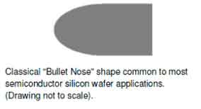
Silicon Wafer to Microchip
After the steps stated on this page, the wafer are then fabricated into microchips. This second step is refered to Wafer Fabrication.
Send us the specs and quantity that you would like us to quote!
Get Your Quote FAST! Or, Buy Online and Start Researching Today!
What is Wafer Preparation in Integrated Circuit (IC) Fabrication?
The most common method for silicon wafer preparation involves preparing a single crystal seed and dipping it into molten silicon. Once in the liquid, the seed is pulled from the molten silicon slowly, while the rod rotates. Then, the finished wafer is polished and has a crystallographically flawless surface. Once cooled, the wafer is ready for further processing, including polishing and etching.
The next step in silicon wafer preparation is to apply a dopant, which are elements from Groups 3 and 4 of the periodic table. These elements are used to alter the properties of the wafer material, such as allowing certain semiconductors to conduct electricity and conduct current. The dopants can be Phosphorus, Boron, Antimony, as well as N-type and P-type semiconductors.
During silicon wafer preparation, the polycrystalline rod is placed in a chamber with controlled amounts of argon. One end of the rod is attached with a single seed crystal. An induction coil is moved along the length of the rod, heating the molten silicon and causing the molten zone to shift. The molten silicon re-solidifies into a single crystal with a desired orientation.
After polishing, silicon wafers are consolidated into process lots and transported to the next step. The next step in silicon wafer preparation involves the application of dopants, elements from Groups 3 and 4 of the periodic table. These elements will affect the properties of the molten silicon. They are known as dopants and can include a wide variety of elements. Some common dopants are Arsenic, Antimony, and Boron.
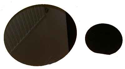
The process begins with the growth of a silicon ingot. This silicon ingot is ground to a rough diameter, and is marked with a notch to indicate orientation. The ingot is then sliced using a diamond edge saw. This type of cutting minimizes damage to the silicon wafer by minimizing thickness variations, bow, and warp defects. It is subsequently cleaned and shipped to the next operation. To ensure that the final product is of high quality, the silicon wafers are inspected for refractivity, abrasion, and corrosion.
After the initial polishing process, the silicon wafers are transported to the next step. They are cleaned and consolidated into process lots, and then they undergo a complex polishing process. After this, the wafers undergo multiple polishing steps. Each step is done to increase the smoothness of the surface. A polishing process will also remove the rough spots and make the surface more planar. This is essential for the flue-line geometries used in the production of ICs.
After the silicon wafers are polished, they are cleaned and dried. Then they are ready for other processing steps. These steps should be done carefully to ensure the purity of the silicon wafers. If the process is not done correctly, the silicon wafers can be contaminated with contaminants, which can make the device useless. These processes are crucial for the production of semiconductor products. The quality of the finished product depends on the quality of the process and the materials used.
To create an effective semiconductor, a freshly sliced silicon wafer must have a mirror-like surface. To do this, the silicon wafers are cleaned and inspected. A diamond edge saw is then used to cut the silicon ingots to reduce the diameter of the final semiconductor. These steps may lead to a defect that prevents a semiconductor from being manufactured. Further, a polishing process can result in a distorted product.
After the silicon wafers have been cleaned, they will undergo a polishing process. This process removes the damaged silicon layers and produces a highly planar surface, which is important for a variety of processes. This is an essential part of silicon wafer preparation and is performed to ensure that the finished product is defect-free. The final polishing step is crucial because it will determine whether the semiconductor will perform properly. Depending on the thickness of the silicon, this stage can lead to an error in the final product.
To prepare a silicon wafer, silicon ingots are circular. The resulting silicon wafer is a single crystal. The ingots are made by dipping the seed crystal in molten silicone and then slowly rotating and extracting the wafers as they grow. To learn how to pronounce the word "wafer," practice making a variety of exaggerated sounds, and recording yourself speaking in full sentences.
Silicon Wafer in Miniaturized Circuit Boards
There's also a miniaturized version of a circuit board inside an integrated circuit : the tracks are created in microscopic form on the surface of a silicon wafer. [16]
With this technique an entire circuit could be "integrated" on a single piece of solid material and an integrated circuit ( IC ) thus created. [20]
In the manufacturing process of IC, electronic circuits with components such as transistors are formed on the surface of a silicon crystal wafer. [8]
The rows of electronic components that make up the integrated circuit are imprinted onto the silicon wafer by various deposition & etching processes. [9]
The basic idea was to take a complete circuit, with all its many components and the connections between them, and recreate the whole thing in microscopically tiny form on the surface of a piece of silicon. [16]
#packaged #transistors
Then the factory "etches" circuits on the silicon wafer and cleans the etched wafer, and places the transistors and other circuits on the chips. [23]
Each chip on the wafer is tested for correct performance and then separated from other chips on the wafer by a saw. [1]
Good chips are placed into the supporting packages that allow them to be plugged into circuit boards, and bad chips are marked and discarded. [1]
Manufacturing chips and microchips involve cutting the wafers into small square or rectangular "chips" or "die ", using a process known as silicon wafer dicing. [3]
The way a chip works is the result of how a chip's transistors and gates are designed and the ultimate use of the chip. [22]
Each layer of the chip is electrically connected to the next with billions of transistors, and each circuit pattern is unique. [5]
#masks #step #beams #hundreds #operation
There are basically two main components to each step - masking off areas to operate on, and then performing some operation on those areas. [11]
Photolithography using different masks, followed by more etching and doping, can be repeated hundreds of times for the same chip, producing a more complex integrated circuit at each step. [1]
The advantage is that no masks are required as the geometry is simply programmed into the machine, however it is much slower as the beam ( or multiple beams ) must trace out each individual feature. [11]
Making chips is a complex process requiring hundreds of precisely controlled steps that result in patterned layers of various materials built one on top of another. [22]
#chuck #flows #deposit
Small gas flows occur during chemical vapor deposition ( CVD ), a process that occurs inside a vacuum chamber when ultra - rarefied gases flow across a silicon wafer to deposit a solid film. [17]
In the Sandia design, the electrostatic chuck face is, itself, an easily produced, patterned silicon wafer that consists of tiny, non - conductive silicon dioxide islands rising above the surface of the rest of the wafer. [2]
A nonconducting layer of silicon dioxide is grown or deposited on the surface of the silicon wafer, and that layer is covered with a photosensitive chemical called a photoresist. [1]
The Sandia chuck, like more conventional ones, confines a thin layer of helium gas that drains heat from a silicon wafer during plasma - etch fabrication steps. [2]
#fuels #pounds #gram #g
For every gram of a microchip, 630 grams of fossil fuels are used, whereas for every gram of an automobile, only 2 grams of fossil fuels are used. [23]
About 0.16 pounds of chemicals are used for each 0.004 pound chip produced, which is about 40 times the weight of the chip. [23]
The total weight of secondary fossil fuel and chemical inputs to produce and use a single 2-gram 32 MB DRAM chip are estimated at 1600 g and 72 g, respectively. [21]
For a 2-gram, 32-megabyte memory chip and its plastic package, about 70.5 pounds of water is used ( Williams, et al, 2002 ). [23]
Use of water and elemental gases ( mainly N2 ) in the fabrication stage are 32,000 and 700 g per chip, respectively. [21]
#quantum #need #Intel
What they do : NUVIA is creating high - performance silicon design for computers that need to keep up powerful computing capacity. [4]
Since it pioneered the manufacturing of silicon transistors, it should come as no surprise that Intel is heavily invested in research into silicon - based quantum computing. [18]
IBM, Google, Intel and others are in a race to create quantum computers with enormous processing power, way more than silicon transistors, using quantum bits, aka 'qubits '. [18]
However, Intel's spin qubit system still only works close to absolute zero; cold computing will go hand in hand with the development of quantum computers. [18]
Who needs the on - off states of a classical computer system when you can have the quantum world's superposition and entanglement phenomena? [18]
#atoms #carbon #element #life
Silicon is also happy to bond powerfully to other silicon atoms ( just like carbon to carbon ) and can thus double - lock certain conformations into place. [10]
It's most commonly found as a silicate ( SiO 4, or one silicon atom bound to four oxygen atoms ) and silica ( SiO 2, or one silicon atom bound to two oxygen atoms ). [10]
However, compared with single - crystal silicon's atomic density of 5x10²² atoms per cm3, this still gives a purity greater than 99.9999 %. [19]
Silicon is also less widely reactive than carbon, meaning silicon - based life could be less chemically diverse, or require a much wider array of reaction - driving silicon enzymes to force chemically less - desirable compounds into existence. [10]
#company #technology #semiconductor #manufacturers
What they do : Infineon is a microchip manufacturer with a focus on developing semiconductor technologies that enable green and energy efficient technology. [4]
What they do : II - VI is a global semiconductor company that develops materials and microchip solutions to support the operations of international companies. [4]
What they do : Alien Technologies develops and manufactures RFID transceiver chips for use by companies to manage inventory and track transportation of items. [4]
Since the 1960s, Silicon Valley has been a gravitational center for the world's semiconductor manufacturers, and the region has built its name on the silicon and integrated circuit technology that makes the rest of the tech world possible. [4]
The computer company and Taiwan Semiconductor Manufacturing Co. went to work on the A12, a 7-nanometer design that's smaller and more efficient than the current 10-nanometer chip. [5]
#dicing #process #mm #diameter
This wafer dicing process allows us to dice silicon and semiconductor wafers as thin as 0.020 mm ( 0.0008 ") and up to 300 mm ( 12.0" ) in diameter with exceptional precision and perfect repeatability. [3]
During the silicon wafer dicing process, the wafers are mounted on dicing tape that secures the wafer to a metal frame. [3]
Syagrus Systems provides world - class post fab processing for silicon wafers and semiconductor wafers, with wafer dicing processes that are customizable to your unique needs. [3]
We offer high magnification, fully - automated, die visual inspection to ensure your wafer is at peak optimization following the wafer dicing process. [3]
Wafers under 200 mm diameter have flats cut into one or more sides indicating the crystallographic planes of the wafer ( usually a { 110 } face ). [19]
#microchip #algorithms #AI #designing
The algorithms inside were developed by iFlytek, but the hardware -- the microchips that bring those algorithms to life -- was designed and made elsewhere. [6]
Instead, its existing strength in AI and its unparalleled access to the quantities of data required to train AI algorithms could give it an edge in designing chips optimized to run them. [6]
Built to be used even by those new to silicon, their accessible online core and chip designing platform enables high speed development and testing of chips and core IP. [4]
The primary building block of our modern computers is the silicon microchip, but what exactly is a microchip and how is it made? [12]
New types of chips are being invented to fully exploit advances in AI, by training and running deep neural networks for tasks such as voice recognition and image processing. [6]
#times #equipment #paragraph
Much of the equipment that these workers use is programmable -- that is, a computer language determines how the equipment operates. [7]
So if you want to build a computer with just enough memory to store this paragraph, you're looking at about 750 characters times 8 or about 6000 switches -- for a single paragraph! [16]
Despite its gargantuan size, it was thousands of times less powerful than a modern laptop -- a machine about 100 times smaller. [16]
Circuit boards are fine in small appliances like this, but if you try to use the same technique to build a complex electronic machine, such as a computer, you quickly hit a snag. [16]
#Moore #Law #years #doubled
According to Moore's Law, the number of transistors on an integrated circuit doubles every two years, leading to an exponential improvement in electronics. [0]
Back in 1965, Gordon Moore, co - founder of Intel, observed that the number of transistors on a one - inch computer chip double every year, while the costs halve. [18]
Chart : Moore's Law : The number of transistors packed into microchips has roughly doubled every year or two for the last five decades -- in other words, it's grown exponentially. [16]
Interviewed by The New York Times 50 years later, in 2015, Moore revealed his astonishment that the law has continued to hold : "The original prediction was to look at 10 years, which I thought was a stretch. [16]
#photoresist #light #exposure #generate #mask
The photoresist is exposed to ultraviolet light shined through a patterned plate, or "mask," which hardens the areas exposed to the light. [1]
Similar to the development of film photographs, the photo - engineering process uses light application and chemical exposure to generate a semiconductor microchip. [13]
The illumination system uses a reduction lens with a pre - programmed exposure time and stepping movement to generate grid pattern. [13]
The feature size that can be projected onto the photoresist coating on the wafer is determined by the wavelength of the light used. [11]
The developed photoresist is used as a mask for etching to process the thin film into the shape of the wiring and other components. [8]
Their specialty is developing photoresists ( the "negatives," or blank wafers on which circuitry is printed ), that are specifically designed for exposure to extreme ultraviolet wavelengths. [14]
#dies #area #cost #DPW
Converting to larger 450 mm wafers would reduce price per die only for process operations such as etch where cost is related to wafer count, not wafer area. [19]
This formula simply states that the number of dies which can fit on the wafer can not exceed the area of the wafer divided by the area of each individual die. [19]
A unit wafer fabrication step, such as an etch step, can produce more chips proportional to the increase in wafer area, while the cost of the unit fabrication step goes up more slowly than the wafer area. [19]
In order to minimize the cost per die, manufacturers wish to maximize the number of dies that can be made from a single wafer; dies always have a square or rectangular shape due to the constraint of wafer dicing. [19]
#bending #UTCs #devices #response #variations
As an example, variations in the output of devices on UTCs could be exploited to predict the state of bending ( e.g., curvature ) or the shape of UTC under bending condition. [15]
This could be achieved by developing models that accurately capture the electro - mechanical variations in the response of devices on UTCs. [15]
Instead of minimizing or cancelling such effects, it could be useful if an alternative strategy is devised to exploit bending induced variations in the response of UTCs. [15]
These stresses induce changes in the band structure and the piezoresistive property of Si, which eventually show up as variation in the electrical response of devices on UTCs. [15]
For complex circuit design in flexible electronics and to predict their response under different bending condition precisely, it is necessary to understand these variations and implement predictive models in electronics design tools.34,35 The variations in device response could be reduced by using suitable compensation techniques in the layout. [15]
#parts #core #CPUs
A small 74mm^2 chip like Zen 2 has a potential of nearly 800 chips per wafer, while Intel's 10-core Skylake - X chips are around 322mm^2 and only fit about 170 chips per wafer. [12]
Sometimes you can get lucky and win the silicon lottery with a great chip sold as a second - tier part. [12]
In the past, it was sometimes possible to reverse the downgrading -- AMD had 2-core and 3-core CPUs in the past where you could potentially turn them into a working 4-core part if you got lucky. [12]
After binning and harvesting of chips, sometimes a company will simply have too many 'good' chips and not enough 'lesser' chips. [12]
If there aren't enough' bad 'chips available, some of the higher quality parts get downgraded and sold as a less expensive part. [12]
#Si #thickness #bulk #UTCs
The heat dissipation, particularly in the UTCs realized from SOI wafers having top Si thickness in the nanoscale, significantly differ from conventional bulk Si based chips. [15]
Therefore, for practical purposes the fundamental electrical properties of ultra thin Si remains unchanged when they are realized by thinning bulk Si. [15]
The nanometre range is hard to achieve with mechanical grinding or wet etching of bulk Si wafer, nonetheless with SOI wafers it is possible to obtain UTCs with nanometre thickness. [15]
To reach < 50 um, the thickness of a conventional bulk wafer or SOI wafer undergoes thinning process, which is known to induce stress in Si. [15]
For Si, the h b is about 80 nm and this value depends on parameters such as in - plain strain, Poisson's ratio and the Young's modulus of bulk Si. [15]
Sources:
[0]: http://www.itnews.com.au/news/mits-hybrid-microchip-to-overcome-silicon-size-barrier-156309
[1]: https://www.computerworld.com/article/2576786/making-microchips.html
[2]: https://www.sandia.gov/media/chuck.htm
[3]: https://www.syagrussystems.com/wafer-dicing
[4]: https://www.builtinsf.com/2020/02/14/silicon-valley-microchip-companies
[5]: https://www.tomorrowsworldtoday.com/2019/01/04/making-a-microchip/
[6]: https://www.technologyreview.com/2018/12/14/138260/china-has-never-had-a-real-chip-industry-making-ai-chips-could-change-that/
[7]: https://www.truity.com/career-profile/semiconductor-processor
[8]: https://www.hitachi-hightech.com/global/products/device/semiconductor/process.html
[9]: https://www.sciencesource.com/archive/Light-Micrograph-of-a-silicon-wafer-microchip-SS2168614.html
[10]: https://www.extremetech.com/extreme/208501-what-is-silicon-and-why-are-computer-chips-made-from-it
[11]: https://electronics.stackexchange.com/questions/134365/how-are-microscopic-transistors-on-microchips-made
[12]: https://www.pcgamer.com/how-are-microchips-made-anyway/
[13]: https://multisourcemfg.com/2020/07/12/microchip-reticle-handling-semiconductor-components/
[14]: https://www.corvallisadvocate.com/2020/osu-spin-off-company-gets-31-million-for-microchip-work/
[15]: https://www.nature.com/articles/s41528-018-0021-5
[16]: https://www.explainthatstuff.com/integratedcircuits.html
[17]: https://sst.semiconductor-digest.com/2018/08/helping-the-microchip-industry-go-very-low-with-the-flow/
[18]: https://www.techradar.com/news/silicon-chips-are-reaching-their-limit-heres-the-future
[19]: https://en.wikipedia.org/wiki/Wafer_(electronics)
[20]: https://www.britannica.com/technology/integrated-circuit
[21]: https://pubmed.ncbi.nlm.nih.gov/12521182/
[22]: https://www.intel.com/content/www/us/en/history/museum-making-silicon.html
[23]: https://enviroliteracy.org/environment-society/life-cycle-analysis/computer-chip-life-cycle/
What are the Steps for Preparing Silicon Wafers?
There are several stages to make a silicon wafer that are used to fabricate semiconductor devices . First the silicon is mined from beach sand! There are only a few beaches in the world where you can mine the sand.
What is Silicon Crystal Growth?What is Silicon Crystal Growth? This process is a simple one. A growing crystal is composed of cubic particles on a simple cubic lattice. Only ten of the sixteen positions are filled with particles, and only the top layer is completely solid. As a particle joins the crystal, it will interact with its three neighbors, forming a single, low-oxygen crystal. This is a very complex process, but it works well. In order to grow single crystals, scientists use a technique called the Bridgman method. This technique makes use of a conical crucible that has a lower conical end. This crucible is placed over a heat source, which maintains the molten state. As crystals grow, the conical tip of the crucible is gradually lowered, at a rate that corresponds with the growth rate of the crystal. This process creates one single large crystal from the molten material. |

Polysilicon chunks are poured into a crucible. A silicon seed crystal is grown into a respective diameter. |
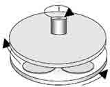
Single Crystal Silicon IngotA single crystal silicon ingot is a semiconductor made from a single crystal of silicon. It is typically grown as a large cylindrical ingot. This material is then ground and etched to achieve the required diameter. It is then cut into blocks of a specific length and given a notch, primary flat, and secondary flat to ensure optimal conductivity and orientation. This process is known as sintering, and can be automated, using a wafer handling system. To make a silicon ingot, polycrystalline silicon is purified to a few parts per billion. The polysilicon is then melted at 1420°F. Phosphorus and boron are added to the molten silicon to balance electrical resistance. A seed crystal silicon rod is placed over the molten silicon and etched so that all transistors align to the same orientation. The finished ingot is cut into chips. Silicon ingots are commonly manufactured using the Czochralski crystal growth process. Virgin polycrystalline silicon is melted in a quartz crucible, dopants are added, and a seed crystal is lifted from the melt, forming a monocrystalline ingot. |

The seed crystal is grown into a silicon ingot. |
What is Silicon Crystal Trimming and Diameter Grind?
The cutting process uses a wire saw to cut the ingot into blocks. The peripheral surface is ground to the required diameter, and flats or notches are added to indicate crystallographic orientation. Laser grinding may be used for high-precision slicing. Large wafers are typically cut with a rotating diamond inner-peripheral blade, whereas smaller wafers may be sliced using a rotary wire saw. |
 Excess silicon is trimmed and ground down.
|
What is Silicon Flat Grinding?Surface grinding creates a smooth, flat wafer surface. After slicing, wafers are rotary ground to final shape. This step smooths rough edges and reduces stress. Diamond abrasives remove pits and improve ductility and surface quality. Center-site grinding improves uniformity and lowers electrical resistivity. Grinding uses abrasives of varying hardness depending on material removal requirements. |
 Orienting flats are ground into the wafer according to semiconductor standards.
|
What is Silicon Wafer Slicing?Silicon wafers are sliced from large ingots using precision wire saws or lasers. Cooling water removes debris and prevents contamination. Lapping is performed to remove saw marks and relieve mechanical stress. Wafers are etched to eliminate microscopic cracks. Edge rounding follows to reduce chipping and breakage during device fabrication. |
 Ingots are sliced into wafers at thicknesses chosen by the operator.
|
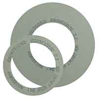
Silicon Edge Rounding Guide
The technique improves visibility and precision and can be applied to many substrate types including AlN, fused silica, glass, and quartz. |
 loading="lazy"
Wafer flats are rounded to increase strength. loading="lazy"
Wafer flats are rounded to increase strength.
|
What is Silicon Wafer Lapping?
|
What is Silicon Wafer Etching?
Dry etching removes oxide layers. Anisotropic etching with KOH creates directional features essential for MEMS and IC fabrication. |
What is Silicon Wafer Polishing?
|
What is Silicon Wafer Inspection?
|
 The process begins with a fully grown silicon ingot that is ground to a rough diameter and given a notch to indicate orientation.
Edge grinding is performed with a diamond saw, minimizing wafer damage and reducing bow and warp.
The process begins with a fully grown silicon ingot that is ground to a rough diameter and given a notch to indicate orientation.
Edge grinding is performed with a diamond saw, minimizing wafer damage and reducing bow and warp.
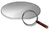
 Edge rounding produces uniform circular edges, improving wafer strength and reducing chipping.
This is essential for stable handling during semiconductor processing.
Edge rounding produces uniform circular edges, improving wafer strength and reducing chipping.
This is essential for stable handling during semiconductor processing.
 Silicon wafer lapping removes TTV (total thickness variation) and improves wafer flatness. It prepares wafers for further polishing and etching.
 Etching removes thin layers of silicon using chemical processes such as phosphoric acid at high temperatures. Water-to-acid ratios must be precise to prevent explosive reactions.
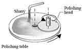 Polishing removes microcracks and creates a mirror-like finish required for device fabrication. CMP (Chemical Mechanical Polishing) delivers the final precision surface.
 After slicing and lapping, wafers are cleaned, etched, stress-relieved, and edge-rounded to reduce breakage.
 Inspection identifies defects using optical scanning, dark-field imaging, and defect mapping. This ensures wafers meet production standards.
 Advanced inspection tools compare cell-to-cell and die-to-die patterns to detect pits and contamination.