
Understanding Silicon Wafer Thickness Standards
Silicon wafer thickness standards help ensure that wafers have the mechanical stability and dimensional consistency required for semiconductor fabrication, laboratory research, MEMS processing, photolithography, thin-film deposition, and other wafer-based processes. Although silicon wafers can be manufactured in many custom thicknesses, commonly used wafer diameters are associated with nominal thickness ranges that are compatible with established handling and processing equipment.
In general, the nominal thickness of a silicon wafer increases as wafer diameter increases. Larger wafers require sufficient mechanical rigidity to reduce the risk of excessive deflection or breakage during handling and processing. For example, commonly encountered thicknesses are approximately 275–280 µm for 50.8 mm (2-inch) wafers, about 525 µm for 100 mm (4-inch) wafers, about 675 µm for 150 mm (6-inch) wafers, about 725 µm for 200 mm (8-inch) wafers, and about 775 µm for 300 mm (12-inch) wafers. Actual specifications can differ depending on wafer type, supplier, application, and applicable standard.
Why Does Silicon Wafer Thickness Increase with Diameter?
As the diameter of a wafer increases, maintaining adequate rigidity becomes increasingly important. A larger wafer with insufficient thickness is more susceptible to mechanical deflection and damage during handling. For this reason, silicon wafer diameter and thickness are typically considered together when selecting a substrate.
Wafer thickness can also affect compatibility with processing equipment such as wafer chucks, carriers, robotic handling systems, lithography tools, grinding equipment, and bonding systems. Researchers should therefore select a wafer based on the complete dimensional specification rather than diameter alone.
Nominal Thickness vs. Thickness Tolerance
Nominal wafer thickness is the target thickness specified for a wafer, while thickness tolerance defines the permitted deviation from that target. For example, a wafer specified as 525 ± 15 µm has a nominal thickness of 525 µm and an allowable thickness range defined by the ±15 µm tolerance.
Thickness tolerance should not be confused with Total Thickness Variation (TTV). TTV describes the difference between the maximum and minimum local thickness measured across a wafer. A wafer can therefore meet its overall thickness specification while still having a separate TTV requirement controlling thickness uniformity across its surface.
Why Total Thickness Variation Matters
Low TTV is particularly important in processes that require high dimensional uniformity. Applications such as photolithography, wafer bonding, MEMS fabrication, precision micromachining, and some advanced packaging processes can benefit from substrates with tightly controlled thickness variation.
UniversityWafer supplies low-TTV silicon wafers for applications requiring tighter thickness uniformity, including selected substrates with TTV specifications in the low-micrometer range.
Standard vs. Custom Silicon Wafer Thickness
Standard thickness wafers are useful when compatibility with established semiconductor equipment is important, but research and specialized device fabrication may require non-standard dimensions. Silicon substrates can be produced or processed to achieve thinner or thicker configurations depending on the application.
Thin silicon wafers are used in applications such as MEMS, sensors, flexible or lightweight devices, and advanced packaging research. Thickness reduction may involve processes such as grinding, lapping, and polishing. As wafers become thinner, careful handling becomes increasingly important because their resistance to mechanical damage is reduced.
When ordering a silicon substrate, researchers should specify not only the required wafer diameter and thickness, but also relevant parameters such as thickness tolerance, TTV, crystal orientation, resistivity, dopant type, surface finish, and whether the wafer requires single-side or double-side polishing.
Get Your Silicon Wafer Quote FAST!
Or, Buy Wafers Online
and Start Researching Today!
How to Choose the Correct Silicon Wafer Thickness
Selecting the correct silicon wafer thickness depends on more than wafer diameter alone. The substrate must have sufficient mechanical stability for handling while also meeting the dimensional requirements of the intended fabrication process. Standard-thickness wafers are appropriate for many semiconductor and research applications, while specialized processes may require thinner, thicker, or more tightly controlled substrates.
Researchers should consider wafer diameter, nominal thickness, thickness tolerance, Total Thickness Variation (TTV), bow, warp, surface finish, and equipment compatibility before selecting a substrate. These geometric specifications can become especially important in precision lithography, wafer bonding, MEMS fabrication, and other processes requiring controlled wafer geometry.
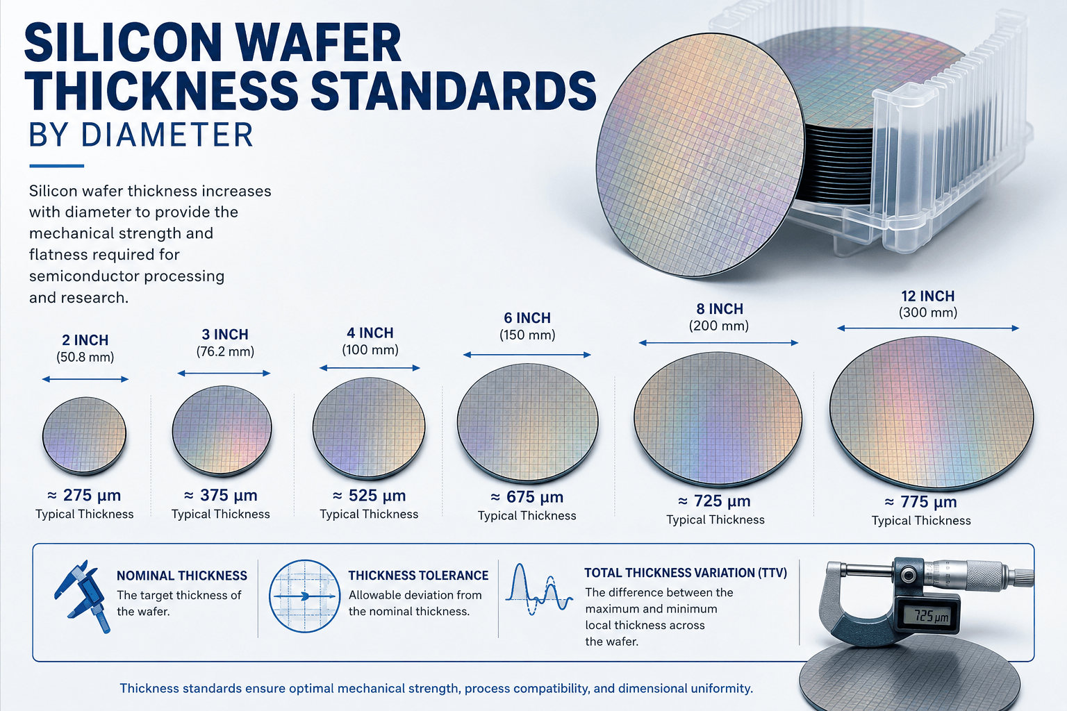
Common Silicon Wafer Diameter and Thickness Combinations
Standard or commonly encountered wafer thickness generally increases with diameter. The following values provide useful reference points for frequently used silicon wafer sizes:
- 2 inch (50.8 mm): approximately 275–280 µm
- 3 inch (76.2 mm): approximately 375–381 µm
- 4 inch (100 mm): approximately 525 µm
- 5 inch (125 mm): approximately 625 µm
- 6 inch (150 mm): approximately 675 µm
- 8 inch (200 mm): approximately 725 µm
- 12 inch (300 mm): approximately 775 µm
These values should be treated as common reference dimensions rather than mandatory thicknesses for every wafer. Custom and non-standard thicknesses are widely used in research and specialized fabrication, and the required specification should always be confirmed for the specific process and equipment.
Thin Silicon Wafers
Thin silicon wafers can be useful when reduced substrate thickness is required for MEMS, sensors, advanced packaging, device thinning, or specialized research. Silicon wafers can be thinned after initial wafer production using processes such as grinding, lapping, polishing, or combinations of these techniques.
As a silicon substrate becomes thinner, its mechanical rigidity decreases and the risk of breakage, bowing, and handling damage generally increases. Very thin wafers may therefore require specialized carriers, temporary bonding, or carefully controlled processing conditions.
Silicon Wafer Backgrinding and Thickness Reduction
Silicon wafer backgrinding is commonly used to remove material from the backside of a wafer and reduce its overall thickness. Grinding can provide substantial material removal, while subsequent processes such as polishing may be used when tighter surface or geometric specifications are required.
When specifying a thinned wafer, the final thickness should be considered together with thickness tolerance, TTV, bow, warp, edge condition, and surface finish. The appropriate combination depends on how the wafer will be handled and processed after thinning.
Single-Side vs. Double-Side Polished Wafers
Single-side polished (SSP) silicon wafers are suitable for many processes where only one high-quality polished surface is required. They are commonly used for general semiconductor processing, deposition, lithography, and research.
Double-side polished (DSP) silicon wafers have both major surfaces polished and are useful when both sides participate in processing or when tighter wafer geometry is required. DSP substrates are frequently selected for MEMS, wafer bonding, optical applications, precision metrology, and processes requiring low TTV.
TTV, Bow, and Warp Are Different Specifications
Wafer thickness alone does not fully describe substrate geometry. Total Thickness Variation (TTV) measures the difference between the maximum and minimum local thickness across a wafer. A low-TTV substrate therefore has more uniform thickness across its usable area.
Bow and warp, however, describe aspects of wafer shape rather than local thickness variation. These parameters should not be used interchangeably with TTV. Applications requiring precise focusing, bonding, alignment, or dimensional control may need limits on several of these specifications simultaneously.
Thickness for MEMS and Microfabrication
In MEMS and microfabrication, substrate thickness can influence mechanical behavior and the available depth for structures such as cavities, channels, membranes, and through-wafer features. The correct thickness therefore depends on both the device design and the fabrication sequence.
Crystal orientation can also be important when silicon is anisotropically etched. For example, silicon wafer orientation affects crystallographic etch behavior and should be specified independently of wafer thickness.
What to Specify When Ordering Silicon Wafers
A complete silicon wafer specification should normally include more than diameter and thickness. Depending on the application, researchers may need to define:
- Wafer diameter and nominal thickness
- Thickness tolerance and TTV
- Bow and warp requirements when relevant
- Crystal orientation, such as (100), (110), or (111)
- Conductivity type and dopant, such as p-type boron or n-type phosphorus
- Resistivity range
- Growth method, such as Czochralski (CZ) or Float Zone (FZ)
- Surface finish, including SSP or DSP
- Edge configuration, including flats or notch where applicable
Defining these parameters together helps ensure that the silicon substrate is compatible with the intended fabrication process, measurement technique, and wafer-handling equipment.
Standard and Custom Thickness Silicon Wafers
UniversityWafer supplies silicon substrates in standard and non-standard thicknesses for semiconductor research, MEMS, microfabrication, thin-film processing, wafer bonding, sensors, optics, and other R&D applications. Researchers who require unusual thicknesses or tighter geometric tolerances should specify the required final thickness, tolerance, TTV, diameter, orientation, resistivity, and surface finish when requesting a quote.
Related Silicon Wafer Resources
- Silicon Wafer Diameters and Sizes – Learn about common silicon wafer diameters, dimensions, and standard specifications.
- Total Thickness Variation (TTV) – Understand how TTV measures thickness uniformity across a semiconductor wafer.
- Low-TTV Silicon Wafers – Explore silicon substrates with tightly controlled thickness variation for precision applications.
- How Thin Can Silicon Wafers Be? – Learn about thin silicon substrates, thickness reduction, and handling considerations.
- Silicon Wafer Backgrinding – Discover how backgrinding is used to reduce silicon wafer thickness.
- Double-Side Polished Silicon Wafers – Learn about DSP silicon substrates for MEMS, bonding, metrology, and precision processing.
- Single-Side Polished Silicon Wafers – Explore SSP silicon wafers for semiconductor fabrication and laboratory research.
- Silicon Wafer Crystal Orientation – Compare common silicon crystal orientations including (100), (110), and (111).
- Czochralski Silicon Growth Process – Learn how CZ silicon crystals are grown and processed into semiconductor wafers.
- What Is a Silicon Wafer? – Review silicon wafer properties, manufacturing, specifications, and applications.