
What Is the Czochralski Process?
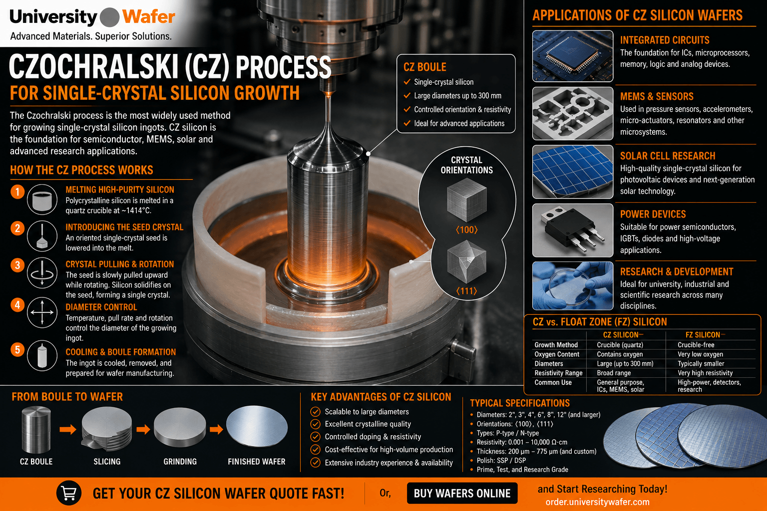
The Czochralski process (CZ process) is a crystal-growth technique used to manufacture large, high-quality single-crystal silicon ingots. These cylindrical crystals, often called boules, are subsequently sliced, ground, polished, and processed into silicon wafers for semiconductor fabrication and scientific research.
Czochralski-grown silicon is widely used because the process enables manufacturers to control crystal diameter, orientation, conductivity type, and dopant concentration while producing large single-crystal ingots suitable for commercial wafer manufacturing.
How Does the Czochralski Process Work?
The CZ process begins with high-purity polycrystalline silicon that is melted inside a quartz crucible at temperatures above silicon's melting point of approximately 1414°C. A precisely oriented single-crystal seed is brought into contact with the molten silicon and then slowly withdrawn while rotating.
As the seed is pulled upward, molten silicon solidifies at the crystal interface and adopts the crystallographic orientation of the seed. Careful control of temperature, pulling speed, and rotation allows a cylindrical single-crystal silicon ingot to form.
1. Melting High-Purity Silicon
High-purity polycrystalline silicon is loaded into a quartz crucible and heated until it becomes molten. Dopants can be introduced into the melt when specific electrical properties are required in the finished crystal.
2. Introducing the Seed Crystal
A small, precisely oriented single-crystal silicon seed is lowered until it contacts the surface of the molten silicon. The seed determines the crystallographic orientation of the growing ingot.
3. Crystal Pulling & Rotation
The seed crystal is slowly pulled upward while the seed and/or crucible rotates. Silicon atoms solidify onto the seed and continue its crystal lattice, gradually producing a cylindrical single-crystal boule.
4. Diameter Control
Crystal diameter is controlled primarily through the thermal conditions and pulling rate. Maintaining stable growth conditions is essential for producing a uniform ingot suitable for subsequent wafer manufacturing.
5. Cooling & Wafer Preparation
After crystal growth is complete, the silicon ingot is cooled and prepared for wafer manufacturing. The boule can then undergo diameter grinding, crystallographic orientation identification, slicing, edge shaping, lapping, etching, cleaning, and polishing.
From Silicon Ingot to Wafer
A CZ-grown silicon boule must undergo several precision-processing steps before it becomes a semiconductor wafer. The ingot is sliced into thin discs, after which the surfaces are processed to achieve the required thickness, flatness, and surface finish.
Depending on the application, finished wafers may be supplied as single-side polished (SSP), double-side polished (DSP), or with additional layers and processing. Some applications may also require silicon wafer backgrinding to reduce the substrate to a specific final thickness.
Doping During CZ Silicon Growth
Electrical properties can be controlled by adding carefully selected dopants to the molten silicon. This enables the production of p-type and n-type CZ silicon wafers with resistivity ranges suited to different semiconductor applications.
Common dopants include:
- Boron: Commonly used to produce p-type silicon.
- Phosphorus: Commonly used to produce n-type silicon.
- Arsenic: Used for certain heavily doped n-type applications.
- Antimony: Another dopant option for specialized n-type silicon.
Crystal Orientation
The seed crystal determines the crystallographic orientation of the growing silicon ingot. Two common orientations for semiconductor wafers are <100> and <111>.
Crystal orientation can influence oxidation, etching behavior, surface properties, device fabrication, and mechanical characteristics. Researchers should therefore select an orientation compatible with their intended process and device architecture.
Oxygen in Czochralski Silicon
One important characteristic of conventional CZ silicon is the presence of interstitial oxygen. During crystal growth, interaction between molten silicon and the quartz crucible introduces oxygen into the melt, some of which becomes incorporated into the growing crystal.
Oxygen can influence the mechanical and electrical behavior of silicon and may be useful or undesirable depending on the application. For research requiring very low oxygen concentration or extremely high resistivity, Float Zone (FZ) silicon may be preferred.
CZ vs. Float Zone Silicon
The primary difference between Czochralski and Float Zone silicon is the crystal-growth method. CZ silicon is grown from molten silicon contained in a crucible, while the Float Zone process uses a localized molten zone without a crucible.
This difference results in several practical considerations:
- CZ silicon: Widely available, scalable to large diameters, and suitable for a broad range of semiconductor applications.
- FZ silicon: Typically has lower oxygen content and can achieve very high resistivity.
- CZ wafers: Commonly used for integrated circuits, MEMS, sensors, and general semiconductor fabrication.
- FZ wafers: Often selected for high-power, high-resistivity, detector, and specialized research applications.
Applications of CZ Silicon Wafers
The scalability and versatility of Czochralski crystal growth make CZ silicon wafers suitable for a wide variety of technologies, including:
- Integrated circuits and microelectronics
- MEMS and microsystems
- Semiconductor sensors
- Power semiconductor research
- Photovoltaic and solar-cell development
- Thin-film deposition
- Oxidation and diffusion experiments
- University and industrial semiconductor R&D
Researchers may also use CZ substrates for silicon epitaxy, thermal oxidation, deposition, lithography, and other semiconductor fabrication processes.
Selecting CZ Silicon Wafers
When selecting a Czochralski-grown silicon wafer, researchers should consider specifications such as:
- Wafer diameter
- Crystal orientation
- p-type or n-type conductivity
- Dopant species
- Resistivity
- Wafer thickness
- Single-side or double-side polishing
- Surface roughness and finish
- Oxygen concentration requirements
- Prime, test, or research-grade requirements
Get Your Czochralski (CZ) Silicon Wafer Quote FAST! Or, Buy Wafers Online and Start Researching Today!
Czochralski Silicon Wafer Applications
Czochralski-grown silicon wafers are used throughout semiconductor manufacturing because the CZ process can produce large-diameter, single-crystal substrates with controlled orientation, conductivity, and resistivity. These wafers provide the foundation for microelectronics, MEMS, sensors, photovoltaic devices, and a wide range of research applications.
Integrated Circuits & Microelectronics
CZ silicon is widely used as a starting substrate for integrated circuits and microelectronic devices. The wafer provides a crystalline platform on which transistors, dielectric layers, metal interconnects, and other microscopic structures can be fabricated.
Typical semiconductor applications include:
- Integrated circuits (ICs)
- Microprocessors and logic devices
- Memory-device research
- Analog semiconductor devices
- Discrete electronic components
- Semiconductor process development
MEMS & Sensor Fabrication
CZ silicon wafers are also used to fabricate MEMS and sensor structures. Silicon's mechanical properties and compatibility with established microfabrication techniques allow researchers to create microscopic mechanical and electronic components on the same substrate.
Applications can include pressure sensors, accelerometers, resonators, micro-actuators, thermal sensors, and other microsystems.
Solar Cell Research
Crystalline silicon produced using the Czochralski method is important in photovoltaic and solar-cell technology. Single-crystal silicon provides a highly ordered crystal structure suitable for investigating efficient photovoltaic devices and related energy-conversion technologies.
Researchers developing photovoltaic devices can explore additional silicon wafers for solar-cell research.
CZ Silicon for Epitaxial Growth
Czochralski-grown substrates can serve as starting wafers for silicon epitaxy. An epitaxial layer with controlled thickness, doping, and electrical properties can be grown over the crystalline substrate to create specialized device structures.
Learn more about silicon epitaxial wafers and their use in semiconductor device development.
Thermal Oxidation & Dielectric Layers
CZ silicon wafers are compatible with thermal oxidation, allowing silicon dioxide (SiO2) to be grown directly on the wafer surface. Thermal oxide can function as an electrical insulator, masking layer, surface passivation layer, or dielectric within semiconductor structures.
Researchers requiring oxide-coated substrates can explore thermal oxide silicon wafers.
Wafer Diameter & Crystal Growth
One major advantage of the Czochralski process is its ability to produce relatively large, uniform single-crystal silicon ingots. During growth, careful control of temperature and pulling conditions determines the diameter of the boule that will eventually be sliced into wafers.
After growth, the ingot undergoes precision processing to establish the required diameter, orientation, thickness, edge geometry, and surface quality.
Controlling Silicon Resistivity
The electrical resistivity of CZ silicon is primarily controlled through the concentration and type of dopant incorporated into the crystal. Selecting the appropriate resistivity is important because it affects electrical conduction through the substrate and its suitability for different devices.
Researchers should specify both the required conductivity type and resistivity range when selecting CZ wafers.
P-Type vs. N-Type CZ Silicon
Czochralski silicon can be manufactured as either p-type or n-type material. P-type silicon is commonly produced using boron, while phosphorus, arsenic, or antimony may be used to create n-type material.
The appropriate conductivity type depends on the intended semiconductor structure, fabrication process, and electrical characteristics required from the finished device.
CZ <100> Silicon Wafers
<100> oriented silicon is widely used in semiconductor fabrication. This orientation is compatible with many oxidation, lithography, transistor, MEMS, and surface-processing techniques.
It is a common choice for integrated circuits and research applications requiring standard semiconductor-processing compatibility.
CZ <111> Silicon Wafers
<111> oriented silicon has different atomic surface arrangements and etching behavior than <100> silicon. These characteristics can be useful in specialized MEMS, anisotropic etching, epitaxial, and materials-science applications.
Oxygen: An Important CZ Characteristic
Because conventional CZ growth uses a quartz crucible, oxygen can enter the silicon melt and become incorporated into the growing crystal. This is one of the key material differences between conventional Czochralski and Float Zone silicon.
Oxygen is not necessarily undesirable. Its presence can influence mechanical strength, defect behavior, and semiconductor processing. The appropriate oxygen concentration therefore depends on the intended application.
When Should You Choose Float Zone Silicon?
For applications requiring very high resistivity or particularly low oxygen concentration, Float Zone (FZ) silicon may be a better choice. The FZ process does not use a crucible to contain the molten zone, reducing a major source of oxygen contamination.
For general semiconductor processing, however, CZ silicon offers broad availability, established manufacturing infrastructure, and a wide selection of wafer specifications.
Processing CZ Silicon Wafers
After crystal growth and wafer slicing, CZ substrates can undergo additional processing depending on the research application. Available process requirements may include:
- Single-side polishing (SSP)
- Double-side polishing (DSP)
- Thermal oxidation
- Thin-film deposition
- Epitaxial growth
- Surface cleaning
- Backgrinding and thinning
- Custom wafer processing
For applications requiring reduced substrate thickness, silicon wafer backgrinding can be used to remove material from the wafer backside.
Choosing the Right CZ Wafer
When specifying Czochralski silicon wafers, consider the complete fabrication process rather than wafer diameter alone. Crystal orientation, dopant, resistivity, thickness, polishing, oxygen content, surface quality, and additional coatings or processing can all influence experimental results.
Typical specifications to provide include:
- Wafer diameter
- <100> or <111> orientation
- P-type or n-type conductivity
- Dopant
- Resistivity range
- Wafer thickness and tolerance
- SSP or DSP surface finish
- Prime, test, or research grade
- Required oxide or deposited films
- Quantity