Epitaxial Wafers for Semiconductor Research
UniversityWafer supplies standard and custom epitaxial wafers
for semiconductor research, prototype fabrication, device development,
materials characterization, MEMS, photonics, RF electronics, power devices,
sensors, and university laboratories.
Available materials and structures may include
epitaxial silicon wafers
,
multilayer silicon structures,
GaN on SiC
,
GaN on sapphire
,
and epi-ready crystalline substrates for
MBE,
MOCVD,
CVD,
and related epitaxial growth processes.
Research Example: Two-Layer Silicon Epi Wafer
A university researcher requested a custom silicon structure combining a
heavily doped substrate with a more lightly doped epitaxial device layer
for subsequent semiconductor fabrication.
Requested specifications:
- Wafer diameter: 100 mm
- Substrate: Approximately 500 µm n+ silicon
- Substrate dopant: Phosphorus
- Substrate dopant concentration: Approximately 1 × 1019 cm−3
- Epitaxial layer: Approximately 10 µm p-type silicon
- Epi dopant: Boron
- Epi dopant concentration: Approximately 7 × 1015 cm−3
- Front surface: Polished for additional device processing
- Optional backside metallization: Approximately 1.5 µm aluminum
- Quantity: 1–25 wafers
The researcher also requested guidance on whether epitaxial growth,
ion implantation, or a combination of processes would be appropriate
for achieving the required layer structure and doping profile.
Reference #210870
How to Specify an Epitaxial Wafer
Providing complete specifications helps determine whether an existing
epi wafer can meet the application requirements or whether
a custom epitaxial structure is needed.
- Substrate material
- Wafer diameter or dimensions
- Crystal orientation and offcut, if required
- Substrate conductivity type
- Substrate resistivity or dopant concentration
- Epitaxial material and layer sequence
- Epi-layer thickness
- Epi conductivity type
- Dopant species and concentration
- Target epi-layer resistivity
- Surface polish requirements
- Buffer, nucleation, oxide, nitride, or metal layers
- Required quantity
Get Your Epitaxial Wafer Quote FAST!
Or,
Buy Wafers Online
and Start Researching Today!
Sapphire Substrates for Epitaxial Growth
Sapphire wafers
are important crystalline substrates for heteroepitaxial growth because
they provide high-temperature stability, chemical durability, electrical
insulation, and commercially available crystallographic orientations.
Sapphire is widely used as a substrate for III-nitride materials such as
GaN, AlN, AlGaN, and InGaN. It is also investigated as a
crystalline substrate for selected oxide and other thin-film material systems.
Growth methods can include
MOCVD
,
MBE
,
and other deposition techniques depending on the material system.
Crystal orientation is important because the sapphire surface affects
nucleation, epitaxial relationship, film orientation, strain, and resulting
material properties.
Research Example: Epi-Ready A-Plane Sapphire
A university postdoctoral researcher requested cleanroom-packed,
A-plane sapphire
substrates for MBE research.
Requested specifications:
- Material: A-plane sapphire
- Nominal orientation: (11-20)
- Orientation tolerance: ±0.1°
- Diameter: 1 inch
- Thickness: Approximately 0.3–0.8 mm
- Surface finish: Single-side polished
- Packaging: Epi-ready and cleanroom packed
- Quantity: 10 wafers
The researcher also requested:
- 20 × 20 mm A-plane sapphire pieces
- Thickness of approximately 0.3–0.8 mm
- Single-side-polished surfaces
- Quantity: 10 pieces
A primary requirement was obtaining surfaces suitable for the intended
vacuum-growth process while minimizing additional handling and preparation
before loading into the research system.
Reference #101799
What Is Epitaxial Growth?
Epitaxial growth is the growth of a crystalline layer on a
crystalline substrate in which the deposited material maintains a defined
crystallographic relationship with the underlying surface.
Unlike an amorphous film or a randomly oriented polycrystalline coating,
an epitaxial layer has an ordered crystal structure whose orientation is
influenced by the crystalline substrate. This allows engineers to design
semiconductor layers with controlled electrical, optical, structural, and
compositional properties.
Epitaxial layers are used in
semiconductor devices
including integrated circuits, transistors, LEDs, laser diodes,
photodetectors, RF devices, power electronics, solar cells, sensors,
and quantum and nanoscale structures.
Homoepitaxy and Heteroepitaxy
-
Homoepitaxy:
The epitaxial layer and substrate consist of the same semiconductor
material, such as single-crystal silicon grown on silicon.
-
Heteroepitaxy:
The epitaxial layer and substrate are different materials but maintain
a defined crystallographic relationship, such as GaN grown on sapphire
or GaN grown on SiC.
Heteroepitaxial growth requires careful management of factors such as
lattice mismatch, thermal-expansion mismatch, substrate orientation,
interface chemistry, strain, and dislocation formation.
Why Epitaxial Layer Quality Matters
Device performance depends strongly on the structural and electrical
quality of the epitaxial layer. The most important specifications vary by
material system and application, but commonly include:
- Layer thickness and thickness uniformity
- Crystal orientation and epitaxial relationship
- Composition and alloy uniformity
- Dopant concentration and carrier concentration
- Electrical resistivity
- Interface abruptness and quality
- Defect and dislocation density
- Surface morphology and roughness
- Residual strain and wafer bow
Precise control of these parameters allows epitaxial wafers to be engineered
for applications ranging from power electronics and RF devices to
LEDs, photonics, MEMS, sensors, integrated circuits, and advanced materials
research.
Applications of Epitaxial Wafers
Epitaxial growth enables device engineers to create semiconductor regions
with properties that cannot always be achieved using the bulk substrate
alone. Depending on the material system, epitaxial wafers support applications
such as:
-
Power electronics – engineered drift layers and
wide-bandgap structures for high-voltage devices
-
RF and microwave electronics – GaN and III-V
heterostructures for high-frequency transistors
-
LEDs and lasers – multilayer III-V structures with
engineered active regions
-
Photodetectors and photonics – controlled optical
absorption and carrier-transport layers
-
Integrated circuits – controlled silicon doping,
resistivity, and junction structures
-
MEMS and sensors – crystalline device layers with
controlled thickness and electrical properties
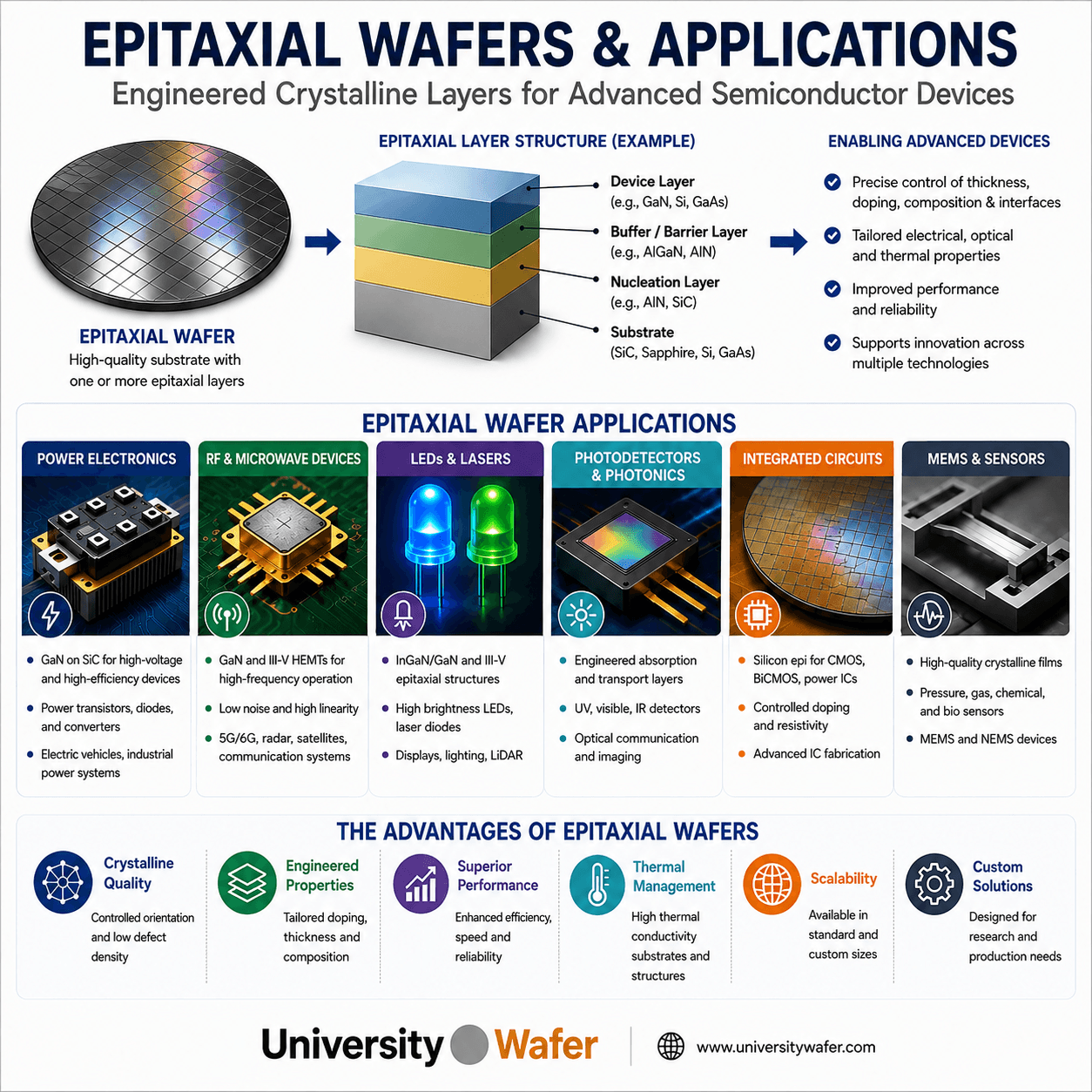
What Is an Epitaxial Wafer?
An epitaxial wafer, often called an epi wafer,
contains one or more crystalline semiconductor layers grown on a crystalline
substrate. During epitaxial growth, the growing layer maintains
a defined crystallographic relationship with the underlying substrate.
Epitaxy enables precise control of semiconductor properties such as
layer thickness, composition, conductivity type, dopant concentration,
resistivity, and heterostructure design. These capabilities make
epitaxial wafers important for integrated circuits, power devices, RF electronics,
LEDs, lasers, photodetectors, sensors, MEMS, and advanced semiconductor research.
UniversityWafer supplies
epitaxial silicon wafers,
GaN on SiC wafers,
GaN on sapphire wafers,
epi-ready substrates, and custom semiconductor structures for research,
device development, and fabrication.
Homoepitaxy vs. Heteroepitaxy
Epitaxial structures are commonly classified as either
homoepitaxial or heteroepitaxial.
-
Homoepitaxy: The epitaxial layer and substrate are the same
semiconductor material. A common example is single-crystal silicon grown
epitaxially on a silicon wafer.
-
Heteroepitaxy: The epitaxial layer and substrate are different
materials but maintain a defined crystallographic relationship. Examples
include GaN on SiC and GaN on sapphire.
In heteroepitaxy, lattice mismatch, thermal-expansion mismatch, surface
preparation, buffer-layer design, and growth conditions can strongly influence
strain, dislocation density, interface quality, and device performance.
Common Epitaxial Growth Methods
The appropriate epitaxial growth technique depends on the substrate,
semiconductor material, required layer thickness, composition, interface
quality, throughput, and intended device.
-
Chemical Vapor Deposition (CVD):
Uses gaseous precursors to form crystalline films and is widely used for
silicon epitaxy and selected compound-semiconductor processes.
-
Metal-Organic Chemical Vapor Deposition (MOCVD):
Widely used for III-V semiconductor heterostructures, including GaN,
AlGaN, InGaN, GaAs, and related materials used in LEDs, RF electronics,
lasers, and power devices.
-
Molecular Beam Epitaxy (MBE):
Uses controlled molecular or atomic beams under ultra-high-vacuum conditions
to grow crystalline layers with precise control of thickness, composition,
doping, and interfaces.
-
Liquid Phase Epitaxy (LPE):
Grows crystalline material from a liquid phase and remains useful for
selected semiconductor and optoelectronic material systems.
GaN/AlN/SiC Epitaxial Wafers
GaN/AlN/SiC epitaxial structures combine gallium nitride
device layers with an AlN nucleation or buffer layer on a
silicon carbide substrate.
AlN can assist GaN nucleation and interface engineering, while SiC provides
high thermal conductivity and is well suited to high-power and high-frequency
semiconductor structures.
GaN/AlN/SiC structures are investigated and used for:
- High-electron-mobility transistors (HEMTs)
- RF and microwave electronics
- High-power semiconductor devices
- GaN materials and interface research
- Surface-science and synchrotron studies
- Advanced wide-bandgap semiconductor development
Research Example: GaN/AlN Epitaxial Structures
A chemical-physics researcher requested 50 mm, on-axis, n-type
GaN/AlN structures on SiC or sapphire for synchrotron radiation research.
- Structure: GaN/AlN/SiC or GaN/AlN/Al2O3
- Diameter: 50 mm
- Orientation: On-axis
- Conductivity: N-type
- GaN thickness: Approximately 0.5–0.8 µm
- AlN thickness: Approximately 0.1 µm
- Quantity: 1 or 5 wafers
Reference #91327
Gallium Nitride Epitaxial Wafers
GaN on SiC
combines wide-bandgap GaN device layers with a substrate that offers high
thermal conductivity. This material platform is important for high-frequency
and high-power electronic devices, including GaN HEMT structures.
GaN on sapphire
is widely used for optoelectronics, particularly LED structures, and is also
used for photodetectors, materials research, and GaN process development.
Research Example: GaN on SiC and Sapphire
A semiconductor company requested:
- GaN on 6H-SiC, 50 mm, on-axis, n-type, with approximately 0.5 µm GaN
- GaN on sapphire, 50 mm, on-axis, n-type, with approximately 0.5–10 µm GaN
- Two-inch 6H-SiC substrates with SSP or DSP surfaces
- Two-inch p-type silicon substrates with double-side polish
Reference #90172
Epitaxial Silicon Wafers
Epitaxial silicon wafers
contain a single-crystal silicon layer grown on a
single-crystal silicon substrate.
The epitaxial layer and substrate can be engineered with different dopant
species, conductivity types, concentrations, and resistivities.
Common silicon epi configurations include:
- N-type epi on an n+ substrate
- P-type epi on a p+ substrate
- P-type epi on an n-type substrate
- N-type epi on a p-type substrate
- Lightly doped or nominally undoped epi layers
- Single-layer and multilayer epitaxial structures
Important specifications include wafer diameter, crystal orientation,
epi-layer thickness, substrate and epi resistivity, dopant species and
concentration, surface finish, layer uniformity, and allowable defect levels.
Research Example: Thin N/N+ Silicon Epi
- Orientation: <111>
- Structure: N-type epi on n+ silicon
- Epi thickness: 500 nm–1 µm
- Target epi resistivity: Approximately 0.1 Ω·cm
- Target substrate resistivity: Less than 0.01 Ω·cm
- Priority: In-stock material and short lead time
Reference #103430
Epitaxial Silicon on SOI Wafers
An epitaxial silicon layer can be grown on the exposed crystalline device
layer of a
silicon-on-insulator (SOI) wafer
when the surface, crystal orientation, thermal budget, and process conditions
are compatible with epitaxial growth.
Epitaxy can increase the crystalline silicon device-layer thickness or create
controlled doping profiles while retaining the buried oxide beneath the
device layer. Such structures may be useful in MEMS, sensors, photonics,
specialized integrated devices, and semiconductor process research.
A researcher requested:
- Approximately 2–4 µm of crystalline silicon
- P-type or n-type conductivity
- An electrically insulating underlying structure
- Small research quantities
- Evaluation of epitaxial growth on silicon-based samples
Reference #94309
PN Junctions in Epitaxial Silicon
A
PN junction
can be created near the interface between an epitaxial layer and substrate
when the two regions have opposite conductivity types. For example, p-type
silicon can be grown epitaxially on an n-type substrate, or n-type silicon
on a p-type substrate.
Epitaxial layer thickness and doping can be engineered to influence the
junction's depletion behavior, electric-field distribution, breakdown
characteristics, and series resistance.
A microstructure-physics researcher requested four-inch silicon wafers
with oppositely doped substrate and epitaxial regions to form a PN junction
near the substrate/epi interface.
Reference #106430
Epitaxial Layers for Transistors and Electronic Devices
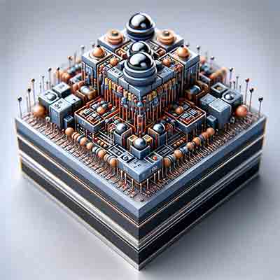
Epitaxy is widely used to engineer semiconductor regions for
bipolar transistors, MOSFETs, power devices, HEMTs, RF electronics,
and integrated circuits. Depending on the device architecture,
epitaxial layers can provide controlled doping profiles, composition,
thickness, strain, and electrical properties.
Benefits of properly engineered epitaxial structures can include:
-
Controlled doping:
Dopant concentration and conductivity type can be tailored across different
regions of the device.
-
Engineered active layers:
Epitaxy allows device layers to be grown with controlled thickness,
composition, and electrical properties.
-
Voltage management:
Lightly doped epitaxial drift regions are commonly used in power devices
to support high electric fields.
-
Heterostructure engineering:
Compound-semiconductor epitaxy enables interfaces such as AlGaN/GaN and
other structures used to control carrier confinement and transport.
Semiconductor Materials Used in Epitaxial Devices
-
Silicon:
Used extensively for integrated circuits, bipolar devices, CMOS-compatible
structures, sensors, and power electronics.
-
Silicon-Germanium (SiGe):
SiGe epitaxy enables band-structure and strain engineering and is widely
used in high-speed SiGe heterojunction bipolar transistors and RF devices.
-
Gallium Arsenide (GaAs):
Used in RF electronics, lasers, LEDs, photodetectors, and other
optoelectronic devices.
-
Gallium Nitride (GaN):
Important for high-power and high-frequency electronics as well as
optoelectronic devices.
Multilayer Epitaxial and Coated Wafer Structures
Semiconductor wafers may combine one or more epitaxial crystalline
layers with separately deposited or grown dielectric, conductive,
or functional films. Not every layer in a multilayer wafer stack is
epitaxial; materials such as SiO2 are typically amorphous rather
than epitaxial.
These engineered wafer stacks can provide controlled electrical,
optical, mechanical, and surface properties at different depths within
the structure.
A researcher requested a structure consisting of:
- Bulk p-type silicon substrate, approximately 0.5 mm thick
-
Approximately 2 µm of higher-conductivity
p-type epitaxial silicon
- Approximately 3.6 µm of silicon dioxide
Reference #103963
LED Epitaxial Wafers
An LED epitaxial wafer contains multiple semiconductor
layers engineered to inject electrons and holes into an active region,
where radiative recombination generates light.
Blue and green LEDs commonly use GaN-based heterostructures containing
InGaN active regions grown on substrates such as
sapphire
or
silicon carbide.
Other III-V material systems based on
GaAs
and related
III-V semiconductors
are used for other wavelength ranges.
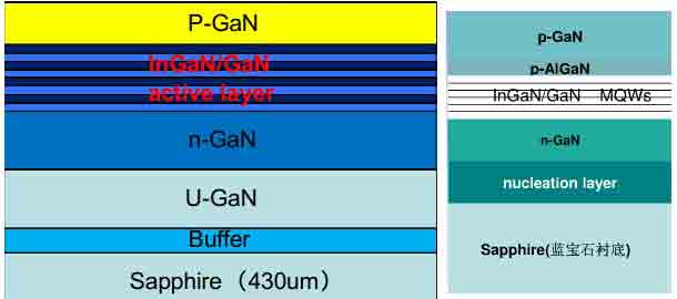
Typical GaN LED Epitaxial Structure
-
Substrate:
Provides mechanical support and the crystalline template for the epitaxial stack.
-
Nucleation or buffer layers:
Help establish the desired crystal structure and accommodate material mismatch.
-
N-type GaN:
Provides the electron-injection side of the LED structure.
-
InGaN/GaN multiple quantum wells:
Form the active light-emitting region in many blue and green LEDs.
-
P-type GaN:
Provides the hole-injection side of the device.
A postdoctoral researcher requested blue or green LED epi wafers with
p-GaN/MQW/n-GaN/u-GaN/sapphire structures, along with undoped and
n-type GaN-on-sapphire materials.
How to Specify an Epitaxial Wafer
Providing complete specifications helps determine whether an existing
epi wafer is suitable or whether a custom epitaxial
structure is required.
- Substrate material
- Wafer diameter or dimensions
- Crystal orientation and required offcut
- Substrate conductivity type and resistivity
- Epitaxial material and complete layer sequence
- Individual epitaxial-layer thicknesses
- Dopant species, conductivity type, and concentration
- Target layer resistivity where applicable
- Surface finish and polish requirements
- Buffer, nucleation, dielectric, or other additional layers
- Required quantity
UniversityWafer supplies standard and custom epitaxial wafers and
substrates for university research, semiconductor process
development, prototype fabrication, device research, and industrial R&D.
Related Epitaxial Wafer Resources
