I am using a laser interferometry to measure my sample piezoelectric response and I just need some piezoelectric material with known d33 (pm/V) piezoelectric coefficients to calibrate my results. Please let me know if you have this by any chance.
Using Laser Iterferometry
A PhD candidate studying in an Advanced Coatings and Surface lab requested a quote for the following.
Reference #131213 for specs and pricing.
Get Your Quote FAST! Or, Buy Online and Start Researching Today!
Silicon Wafers To Measure Coating Thickness Using Interferometry
A Senior Applied Research Scientist requested a quote for the following.
I’ve checked your inventory list for Si wafers and would like to know what the GRADE terms mean e.g. MECH, prime etc.
I am looking to buy some wafers so I can coat them (plasma dep and spin coating) and measure the thickness of the coating applied (using e.g. profilometry, elipsometry or interferometry) or XRF analysis of the coatings for compositional characterisation so I don’t care whether the wafers are N type or P type but care about their flatness.
I am thinking of buying 8” silicon wafers from you and dicing them up myself.
Can you recommend the grade to buy e.g. is MECH grade good enough?
Reference #322246 for specs and pricing.
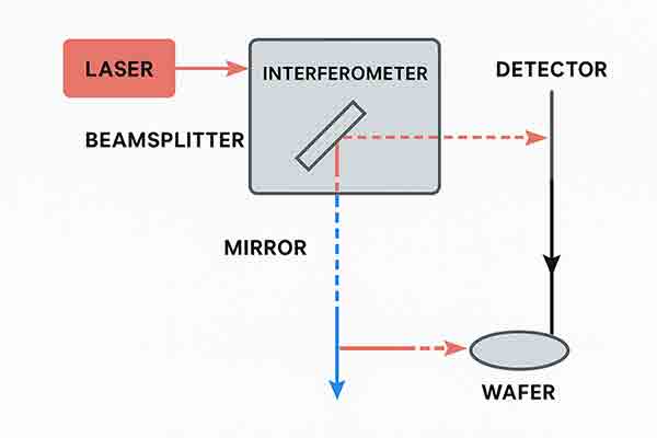
What Is The Importance of Interferometer Measurements?
In semiconductors, an interferometer is an optical device or setup that splits light into two or more paths and then recombines them to produce interference patterns. These interference patterns are sensitive to path length differences on the order of the light's wavelength—making interferometers extremely precise tools for measuring, inspecting, and fabricating semiconductor devices.
📌 What Is an Interferometer?
An interferometer uses the principle of interference—when two or more coherent light waves (often from a laser) overlap, they can constructively or destructively interfere. The resulting pattern contains high-resolution information about the distance, refractive index, or surface shape of materials in the optical path.
🔧 Types Commonly Used in Semiconductors
-
Michelson Interferometer
Used for metrology, alignment, and film thickness measurements. -
Fizeau Interferometer
Ideal for measuring flatness and surface quality of wafers. -
Mach-Zehnder Interferometer
Often used in photonic circuit design and silicon photonics. -
Laser Interferometers
Widely used for positioning systems in lithography and wafer steppers.
🚀 Why Interferometers Are Important in Semiconductors
| Application | Purpose |
|---|---|
| Lithography | Laser interferometers track the position of wafers with sub-nanometer precision during photolithography. |
| Wafer Surface Inspection | Measures flatness, roughness, and thickness variations using Fizeau interferometers. |
| Film Thickness Measurement | Non-contact, high-resolution measurement of thin oxide/nitride layers. |
| Photonic Devices | Used to design and test integrated optical circuits on semiconductor platforms like SOI (Silicon-on-Insulator). |
| Stress and Strain Measurement | Detects warping or thermal stress by analyzing phase shifts in interference patterns. |
| Quantum and Sensing Applications | Interferometers are foundational to high-sensitivity quantum sensors, often built on semiconductor platforms. |
🎯 Summary
Interferometers in semiconductors are essential tools for precise, non-destructive measurements. Whether it's controlling nanoscale movement in photolithography or evaluating the quality of wafer surfaces and thin films, interferometry enables the precision engineering required to build today's microchips and photonic circuits.