
MOCVD — Metal-Organic Chemical Vapor Deposition
Metal-Organic CVD (MOCVD) is the workhorse epitaxy process for III–V and III-N semiconductors. It delivers precise composition control, uniform thickness, and low-defect heterostructures for LEDs, laser diodes, high-electron-mobility transistors (HEMTs), photodetectors, and power electronics. UniversityWafer supports MOCVD R&D and pilot production by supplying prime substrates, epi templates, and reference wafers matched to your process window.
Get ready-to-use substrates and epi templates shipped fast for your GaN, GaAs, or InP growth. Join thousands of labs worldwide that trust UniversityWafer for reliable MOCVD materials.
Get Your Quote FAST! Or, Buy Online and Start Researching Today!
What We Supply for MOCVD Programs
- Substrates: Sapphire (A/C/R), SiC, Si (100/111), GaN-on-sapphire/Si templates, GaAs, InP.
- Epi Templates: GaN/AlGaN buffers, LED templates, GaAs/AlGaAs and InP/InGaAsP platforms for lasers & detectors.
- Process-ready finishes: DSP/SSP, epi-polish, orientation flats, bow/TTV within spec; clean, sealed packaging.
- Documentation: Thickness, TTV/warp, surface roughness, orientation verification; optional XRD/PL/AFM on request.
Common MOCVD Material Systems
- III-N: GaN, InGaN, AlGaN (LEDs, µLEDs, HEMTs, UV optoelectronics)
- GaAs family: GaAs/AlGaAs, InGaAs (lasers, VCSELs, HBTs)
- InP family: InP/InGaAsP, InGaAs (telecom photonics, APDs, EDFAs, high-speed detectors)
Typical Wafer Options
- Diameters: 2″, 3″, 4″, 6″ (select platforms up to 8″)
- Orientations: ⟨0001⟩ (sapphire c-plane), 4H/6H-SiC, Si ⟨111⟩/⟨100⟩; GaAs ⟨100⟩ (± miscut as required)
- Surfaces: Epi-polish, low-Ra; low-bow/low-TTV for uniform growth and wafer handling
Example Epitaxial Stacks We Support
- GaN HEMT: AlN nucleation → step-graded AlGaN/AlN buffers → UID GaN channel → AlGaN barrier → optional p-GaN gate cap.
- Blue/Green LED: GaN nucleation → n-GaN → multiple InGaN/GaN MQWs → p-GaN (with EBL) on sapphire or SiC.
- GaAs/AlGaAs Laser: n-cladding → MQW active region → p-cladding → contact layers on GaAs ⟨100⟩.
- InP Photonics: InP substrate → InGaAsP QW stack → separate confinement layers → InP claddings.
Ordering Checklist
To quote quickly and accurately, include:
- Material + diameter + orientation (e.g., 2″ sapphire c-plane, 4″ SiC, 6″ Si ⟨111⟩)
- Surface finish (SSP/DSP, epi-polish), thickness & TTV/warp limits, bow target
- For templates/epi: target composition, thicknesses, doping, MQW periods, and metrology needs (XRD/PL/AFM/HRXRD)
What Are MOCVD Reactors?
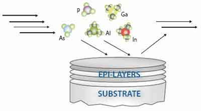
During the growth process of metal-organic crystalline thin films, ultrapurified precursor gases are introduced into a heated reaction chamber called the MOCVD reactor. Inside, a carrier gas—often hydrogen or nitrogen—transports volatile precursors such as trimethylgallium (TMGa), trimethylindium (TMIn), or trimethylaluminum (TMAl) along with hydrides like arsine (AsH₃), phosphine (PH₃), or ammonia (NH₃).
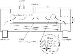
The combination of thermal energy and chemical decomposition causes the desired elements to deposit atom by atom on the wafer surface, forming a crystalline epitaxial layer. Reactor geometries may include horizontal, vertical, showerhead, or planetary types depending on uniformity and wafer size requirements.
Planetary reactors rotate multiple wafers to maintain even gas distribution, while showerhead configurations ensure high uniformity across 2–6 inch wafers. Temperature control, gas flow precision, and exhaust handling are critical for obtaining repeatable and defect-free results. MOCVD reactors are the heart of compound-semiconductor fabrication used in LEDs, HEMTs, and photonic lasers.
Metal-Organic Chemical Vapor Deposition (MOCVD)
Metal-Organic Chemical Vapor Deposition is a key process for creating epitaxial thin films with atomic-level control. It enables the synthesis of III-V and II-VI semiconductor materials like GaAs, InP, InGaAs, AlGaN, and GaN. In this technique, volatile metal-organic compounds react with hydrides under controlled temperature and pressure to form single-crystal films directly on a substrate.
The major advantage of align="center" style="padding: 5px" MOCVD is its ability to control stoichiometry and doping while maintaining smooth interfaces. By adjusting growth parameters such as temperature, pressure, and precursor ratios, users can tailor bandgaps and electrical characteristics for advanced electronic and optoelectronic devices.
Because it operates at relatively low pressures and moderate temperatures, MOCVD is compatible with large wafer diameters, offering uniformity better than ±3% in thickness. Its scalability, high throughput, and precise film quality make it indispensable for research, pilot-line, and full production environments.
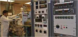
What Are MOCVD Equipment and Components?
A modern MOCVD system integrates advanced subsystems to ensure stable and reproducible growth. Gas delivery panels precisely meter high-purity metal-organics and hydrides using mass-flow controllers. Valved manifolds and heated lines prevent condensation, while dopant channels inject trace gases such as SiH₄ or Cp₂Mg for electrical control.
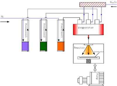
At the core is align="center" style="padding: 5px" the reactor chamber, typically quartz or stainless steel, containing a rotating susceptor heated by RF or infrared elements. The temperature uniformity across the wafer must be tightly controlled to achieve consistent growth rates. Exhaust lines are fitted with scrubbing systems to neutralize toxic byproducts like arsine or phosphine, ensuring safe operation.
Process monitoring tools—reflectometry, pyrometry, or in-situ interferometry—allow operators to track thickness, growth rate, and reflectance in real time. The control software coordinates pressure, flow, and temperature sequences, turning a complex chemical system into a stable manufacturing process. UniversityWafer works with partners providing MOCVD-grown epitaxial wafers that meet stringent semiconductor-industry specifications.
Common Precursors, Dopants, and Growth Chemistry
MOCVD chemistry depends on the selection of volatile precursors that decompose cleanly at the substrate surface. For group-III elements, the most common are TMGa, TMAl, and TMIn, which supply gallium, aluminum, and indium atoms. Group-V elements are usually introduced as hydrides: arsine (AsH₃) for arsenic, phosphine (PH₃) for phosphorus, and ammonia (NH₃) for nitrogen.
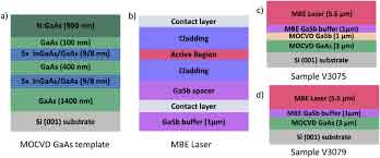 Comparison of MOCVD-grown GaAs templates and MBE laser structures — illustrating buffer, cladding, and active regions.
When heated to 500–800 °C, these gases break apart and deposit atoms in precise ratios, forming compounds like GaAs, InP, AlGaN, or InGaAs. Doping control is achieved through additional gases such as silane (SiH₄) for n-type or cyclopentadienyl-magnesium (Cp₂Mg) for p-type conductivity.
Gas purity and flow stability directly influence film quality. Even trace impurities can change surface morphology or carrier mobility. That’s why MOCVD tools employ ultra-clean lines, bakeable fittings, and real-time gas-leak detection systems for contamination-free epitaxy.
Applications of MOCVD in Advanced Devices
MOCVD enables the controlled fabrication of semiconductor structures used in almost every optoelectronic technology. The process produces LEDs and microLEDs with tailored color wavelengths, laser diodes for optical communications, and VCSELs for 3D sensing and facial-recognition systems. In electronics, MOCVD-grown HEMT and pHEMT devices provide high-frequency performance for radar, RF, and 5G applications.
MOCVD also supports align="center" style="padding: 5px"GaN-on-Si and GaN-on-sapphire power devices, offering efficient energy conversion for automotive and renewable-energy systems. By varying the substrate—GaAs, InP, sapphire, or silicon—engineers can integrate light-emitting, detecting, and amplifying functions on a single platform.
Because of its tunability and scalability, MOCVD continues to drive innovation in displays, photonics, and sensors. UniversityWafer supplies research-grade substrates and epitaxial wafers for universities, national laboratories, and R&D teams exploring next-generation device architectures.