
We would be interested to do on wafer fiber to fiber optical measurements at 1310 or 1550 nm. I already have some questions: - Wafer size: 200 mm. Are you also able to provide 300 mm? - Application: Silicon Photonics - Can you do surface and edge coupling? - What fiber coupling angle can you provide for surface coupling? - What pitch between coupling points can you do to do fiber array measurements? Number of wafer would probably be around 5. If you have discounts at certain quantities let me know.
Substrates Used in Photonics
A photonics engineer requested a quote for the following:
Reference #266691 for specs and pricing.
Get Your Quote FAST! Or, Buy Online and Start Researching Today!
Silicon Wafers for Photonics Waveguide Applications
A material scientist requested the following quote:
I am interested in purchasing 3in wafers of ~330nm SiN on ~3300nm SiO2 all on Si substrate, for photonic applications. If there are wafers in stock that are suitable for photonic/waveguide applications but not of the exact thickness mentioned above, I can also take those because that will arrive sooner. Please send me a quote for 10 wafers and how long they will take to arrive, thank you!
Reference #266490 for specs and pricing.
What is Silicon Photonics?
Silicon Photonics is a technology that involves the use of silicon as a platform for the fabrication of photonic components and devices, such as optical waveguides, modulators, and detectors. It combines the advantages of silicon-based electronics and photonics to create high-speed and high-bandwidth communication systems.
Silicon Photonics relies on the use of integrated circuits (ICs) to manipulate and control light in a manner similar to the way electronic signals are processed in traditional electronic circuits. The key advantage of Silicon Photonics is that it allows for the integration of multiple photonic and electronic components on a single chip, leading to compact and highly efficient systems.
The technology is compatible with the existing CMOS (Complementary Metal-Oxide-Semiconductor) fabrication process, which is used for manufacturing microprocessors and other electronic components. This makes Silicon Photonics a cost-effective solution for high-speed data communication and other photonic applications.
Silicon Photonics has the potential to revolutionize the way data is transmitted and processed in a wide range of applications, including data centers, telecommunications, biomedical imaging, and sensing.
Revolutionizing Photonics: Top Silicon Wafers for Advanced Applications
Silicon wafers are the foundation of photonics, powering high-speed data transmission and cutting-edge sensing technologies. These tiny marvels enable breakthroughs in telecommunications, healthcare, and quantum computing. Let's explore the exciting world of top silicon wafers for photonics applications and see how they're shaping our technological future, changing how we work with light and information at a basic level.
Key Takeaways
- Silicon wafers are essential components in photonic devices, manipulating light at the microscopic level
- Highly doped, Silicon-on-Insulator (SOI), and standard silicon wafers are key types used in photonics
- Ultra-high purity, precise thickness control, and smooth surfaces are crucial features for photonic applications
- Silicon wafers enable advancements in optical communications, sensors, quantum computing, and lidar systems
- The manufacturing process involves crystal growth, slicing, lapping, etching, and polishing stages
- Ongoing research aims to overcome challenges in light emission, heat management, and integration with electronics
Understanding Silicon Wafers in Photonics
Silicon wafers are thin slices of crystalline silicon that form the base for many photonic devices. They're great for controlling light at tiny scales, which is useful for optical communications, sensing, and computing. The crystal structure of silicon is perfect for guiding light waves, allowing the creation of complex photonic circuits that can process information at light speed.
The magic of silicon wafers is in how they guide and control light super precisely. Photonic applications use these wafers to make tiny structures that can control light signals, similar to how electronic circuits control electrical signals. This works because silicon has special optical properties, like how it bends light and doesn't absorb much in the near-infrared range, which is important for telecommunications. By etching really small patterns onto silicon wafers, engineers can make waveguides, resonators, and other photonic parts that are the building blocks of advanced optical systems.
Types of Silicon Wafers for Photonics
There are different types of silicon wafers for photonics, each with special properties for specific uses in optoelectronics:
1. Highly Doped Silicon Wafers
Highly doped silicon wafers are the workhorses of photonic devices. They have extra atoms added to their structure, which changes how they interact with light and electricity. This process, called doping, involves adding impurities like boron or phosphorus to the silicon, which alters its electrical and optical properties.
These wafers are great for making lasers and sensors. They can carry more electricity and interact with light in special ways, which is important for many photonic devices. The high doping levels allow for efficient photodetectors, modulators, and even light-emitting devices when combined with other materials. Being able to adjust the electrical properties of silicon through doping opens up many possibilities for combining electronic and photonic functions on one chip.
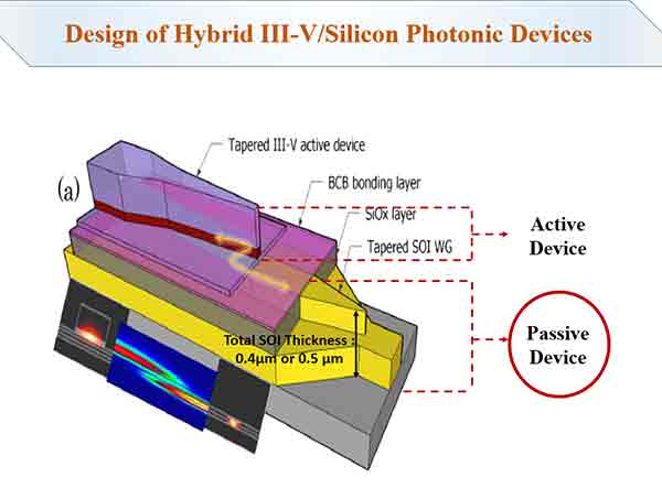
2. Silicon-on-Insulator (SOI) Wafers
Silicon-on-Insulator (SOI) wafers are like sandwich cookies for photonics. They have a thin layer of silicon on top of an insulating material, usually silicon dioxide. This special structure helps control light really well, which is perfect for making tiny optical circuits. The insulating layer stops light from escaping into the base, allowing for very efficient waveguides and other photonic structures.
SOI wafers are used in cool devices like super-fast optical switches and sensors that can detect tiny changes around them. They're important for making photonic devices smaller and more efficient. The unique structure of SOI wafers allows for high-contrast waveguides, which can tightly control light and make photonic circuits smaller. This technology is crucial for developing integrated photonic chips that can handle both optical and electrical signals, paving the way for next-generation computing and communication systems.
3. Standard Silicon Wafers
Standard silicon wafers might sound basic, but they're the workhorses of the photonics world. These wafers come in different sizes and thicknesses, making them useful for various applications. The purity and perfect crystal structure of standard silicon wafers make them a great starting point for many photonic devices.
Standard silicon wafers are often used as a starting point for creating more complex photonic structures. They're like a blank canvas for scientists and engineers to create their photonic masterpieces. These wafers can be processed using many techniques, like photolithography, etching, and deposition, to create intricate photonic structures. They work well with existing semiconductor manufacturing processes, making them good for large-scale production of photonic devices, which helps bring photonics into mainstream technology.
What makes a silicon wafer great for photonics? Let's look at the important characteristics that allow these wafers to excel in photonic applications:
Key Features of Silicon Wafers for Photonics
- Ultra-high purity silicon (99.999% or higher) is essential for optimal optical performance
- Precise thickness control, typically ranging from 300 to 700 micrometers, enables specific photonic applications
- Extremely smooth surface with roughness less than 1 nanometer minimizes light scattering
- Crystal orientation, usually <100>, affects optical and electronic properties
- Low defect density (less than 1 defect per square centimeter) ensures uniform optical behavior
- High transmission in near-infrared wavelengths (90-95% for 700nm-3μm) makes silicon ideal for telecom applications
- Compatibility with existing semiconductor manufacturing processes allows for cost-effective production
- Ability to integrate electronic and photonic components on a single chip enables advanced device designs
- Thermal stability up to 1000°C supports high-power optical applications
- Customizable doping levels allow fine-tuning of electrical and optical properties
These features are crucial for creating photonic devices that can manipulate light with incredible precision. The purer and smoother the wafer, the better it can guide light without losing signal strength. The ultra-high purity ensures that light can travel through the silicon with minimal absorption or scattering, which is essential for maintaining signal integrity in photonic circuits. The precise thickness control allows engineers to design devices that operate at specific wavelengths, crucial for applications like wavelength division multiplexing in optical communications.
The extremely smooth surface is particularly important as it reduces light scattering at interfaces, improving the efficiency of photonic devices. The crystal orientation affects how light interacts with the silicon lattice, influencing properties such as birefringence and nonlinear optical effects. Low defect density is critical for ensuring uniform optical behavior across the entire wafer, which is essential for producing consistent and reliable photonic devices at scale.
Applications of Silicon Wafers in Photonics
Silicon wafers are behind many technologies we use every day. Let's explore some exciting ways these wafers are used in photonics, changing various industries and enabling new technological capabilities:
1. Optical Communications
Silicon wafers are key in optical communication systems. They're used to make tiny devices called optical modulators, which can turn electrical signals into light signals very quickly. This technology lets us send huge amounts of data through fiber optic cables across the world. Silicon photonics enables integrated optical transceivers that can handle data rates of hundreds of gigabits per second, much faster than traditional electronic systems.
Silicon wafers are also used to create other important parts of optical communication systems, like wavelength multiplexers, optical switches, and photodetectors. These integrated photonic circuits are driving the development of next-generation data centers and telecommunications networks, meeting the growing demand for bandwidth in our connected world.
2. Sensors and Detectors
Photonic sensors made with silicon wafers can detect many things, from chemicals in the air to tiny movements. These sensors are used in environmental monitoring and medical devices that can detect diseases early. The high sensitivity and integration capabilities of silicon photonics allow for compact, highly accurate sensing devices.
For example, silicon photonic biosensors can detect specific molecules very sensitively, enabling fast and accurate medical diagnoses. In environmental monitoring, silicon-based optical sensors can measure air and water quality very precisely. The ability to integrate these sensors with electronic readout circuits on the same chip allows for smart, networked sensing systems that can provide real-time data for various applications.
3. Quantum Computing
The strange world of quantum computing also uses silicon wafers. Scientists are using these wafers to create quantum bits, or qubits, which could lead to computers that are much faster than anything we have today. Silicon's long coherence times and compatibility with existing semiconductor manufacturing processes make it good for scaling up quantum computing systems.
Researchers are exploring different ways to create silicon-based qubits, including using the spin of individual electrons in silicon quantum dots or the nuclear spins of phosphorus atoms placed in silicon. The ability to precisely control and manipulate these quantum states using integrated photonic circuits opens up new possibilities for quantum information processing and quantum communication systems.
4. Lidar Systems
Lidar, which stands for Light Detection and Ranging, uses laser light to measure distances. Silicon wafers are used to make the tiny mirrors and sensors in lidar systems, which are important for things like self-driving cars and 3D mapping. Silicon photonics enables compact, high-performance lidar systems that can quickly scan the environment with high resolution.
Advanced silicon photonic lidar systems can include beam-steering capabilities, allowing for fast and precise scanning without moving parts. This technology is not only changing autonomous vehicles but also finding uses in robotics, augmented reality, and industrial automation. The ability to integrate lidar sensors with processing electronics on a single chip is driving the development of smarter and more responsive sensing systems.
Manufacturing Process of Top Silicon Wafers
Creating high-quality silicon wafers for photonics is like baking a really complicated cake. Here's a simplified version of how it's done, with each step carefully controlled to ensure the highest quality and consistency:
1. Crystal Growth: It starts with very pure silicon that's melted and slowly cooled to form a big crystal cylinder called an ingot. This process, called the Czochralski method, involves carefully controlling the temperature and rotation of the growing crystal to ensure uniform properties throughout. The resulting single-crystal ingot can be up to 300mm wide and over a meter long.
2. Slicing: The ingot is then cut into thin wafers, like slicing bread, but much more precisely. Wire saws with diamond-coated wires cut the ingot into wafers as thin as 200 micrometers. This step needs to be very precise to avoid damaging the crystal structure and ensure the wafers are all the same thickness.
3. Lapping: The wafers are smoothed out to make them flat and the right thickness. This uses a mix of abrasive particles to remove tiny bumps from the wafer surface. Lapping helps achieve the exact thickness needed for specific photonic applications and prepares the surface for further processing.
4. Etching: A special chemical bath removes any damage from the slicing process. This step uses a mix of acids or bases to dissolve a thin layer from the wafer surface, removing any leftover damage from the mechanical processes. Etching also helps reveal the pure crystal structure of the silicon, which is essential for its optical properties.
5. Polishing: Finally, the wafers are polished to a mirror-like finish, making them ready for photonic applications. Chemical-mechanical polishing (CMP) is used to achieve an ultra-smooth surface with roughness on the order of angstroms. This final step is crucial for minimizing light scattering and ensuring optimal performance in photonic devices.
Each of these steps is carefully controlled and monitored to ensure the highest quality wafers for photonic applications. Advanced measurement techniques are used throughout the process to check the wafer's properties, including thickness uniformity, surface smoothness, and crystal perfection. The entire manufacturing process takes place in ultra-clean environments to prevent contamination that could affect the wafer's optical and electrical properties.
Challenges and Future Trends
While silicon wafers have revolutionized photonics, there are still some challenges to overcome. Researchers and engineers are working on solutions to push the boundaries of what's possible with silicon photonics:
1. Light Emission
Silicon isn't great at emitting light on its own due to its indirect bandgap. Scientists are working on ways to add other materials to silicon or change its structure to make it better at producing light. Some promising approaches include:
- Integrating III-V semiconductors like indium phosphide with silicon to create efficient light sources
- Exploring germanium-on-silicon structures for light emission in the near-infrared spectrum
- Developing silicon nanostructures that enhance light emission through quantum confinement effects
- Investigating rare-earth doping of silicon to create silicon-based lasers
These advancements could lead to fully integrated silicon photonic circuits that include light sources, modulators, and detectors all on a single chip.
2. Heat Management
As photonic devices get smaller and more powerful, managing heat becomes a big challenge. The high optical power densities in compact photonic circuits can lead to thermal issues that affect device performance and reliability. Researchers are developing new ways to keep these tiny devices cool, including:
- Advanced thermal management materials and structures integrated into silicon photonic chips
- Novel device designs that minimize heat generation and improve heat dissipation
- Active cooling techniques tailored for integrated photonic circuits
- Exploring the use of two-dimensional materials like graphene for heat spreading in photonic devices
Effective heat management is crucial for enabling high-performance, densely integrated photonic systems that can operate reliably in various applications.
3. Integration with Electronics
One of the big goals is to combine photonic and electronic components on the same chip. This could lead to computers that use both light and electricity to process information, making them much faster and more efficient. Challenges in this area include:
- Developing manufacturing processes that are compatible with both electronic and photonic components
- Creating efficient interfaces between optical and electrical domains
- Optimizing chip designs to minimize crosstalk between electronic and photonic elements
- Developing new materials and structures that can serve both electronic and photonic functions
Successful integration of electronics and photonics could revolutionize computing, enabling new architectures for artificial intelligence, high-performance computing, and ultra-fast data processing.
The future of silicon wafers in photonics looks bright. Scientists are exploring new materials and structures to make even better photonic devices. For example, Silicon High Electron Mobility Transistors (HEMTs) are pushing the boundaries of what's possible in high-speed electronic and photonic circuits. These advanced transistor structures combine the benefits of silicon with high-mobility channel materials, enabling faster switching speeds and improved performance in both electronic and photonic applications.
Other exciting trends in silicon photonics include:
- Development of on-chip optical frequency combs for applications in spectroscopy and precision measurement
- Exploration of nonlinear optical effects in silicon for all-optical signal processing
- Integration of plasmonic structures with silicon photonics to enhance light-matter interactions at the nanoscale
- Advancements in silicon photonic packaging and testing to enable large-scale production and deployment of photonic systems
Conclusion
Silicon wafers are the unsung heroes of the photonics revolution. From enabling super-fast internet connections to powering cutting-edge sensors and quantum computers, these tiny slices of silicon are shaping our technological future in amazing ways. The special properties of silicon, combined with years of manufacturing know-how from the semiconductor industry, have made silicon photonics a key technology for the 21st century.
As research continues and manufacturing techniques improve, we can expect to see even more amazing applications of silicon wafers in photonics. The ongoing efforts to overcome challenges in light emission, heat management, and integration with electronics are opening up new possibilities for silicon photonic devices. These advancements could lead to transformative technologies such as:
- Ultra-high-bandwidth optical interconnects for next-generation data centers and supercomputers
- Integrated photonic sensors for environmental monitoring, healthcare diagnostics, and industrial process control
- Quantum photonic circuits for secure communication and quantum information processing
- Neuromorphic photonic systems that mimic the human brain's information processing capabilities
- Advanced lidar and imaging systems for autonomous vehicles and augmented reality applications
Whether it's making our communication networks faster, our medical diagnostics more accurate, or our computers more powerful, silicon wafers will be at the heart of these innovations. The integration of photonics with existing electronic technologies promises to unlock new levels of performance and functionality across a wide range of applications.
The world of photonics is moving fast, and silicon wafers are helping to light the way. As we continue to push the boundaries of what's possible with light and silicon, who knows what incredible technologies we'll see in the future? One thing's for sure: silicon wafers will be there, quietly enabling the next big breakthroughs in photonics. From quantum computing to artificial intelligence, from advanced medical diagnostics to space exploration, the impact of silicon photonics will be felt across industries and scientific disciplines, shaping the technological landscape for generations to come.
What is Photonics Engineering?
Photonics Engineering is the science of using light for energy generation, detection or information transfer. It’s a field that shapes modern medicine, telecommunications, manufacturing and construction products.
Photonics engineers research and develop systems and products based on lasers, optics, fiber optics and imaging. They also test prototypes to verify their ideas before they are perfected for use.
Photonics is the science of light.
Photonics engineering is a field of science and technology that uses light to perform functions traditionally accomplished with electronics. It is an area of research and development centered on the use of light for various technological applications such as communications, information processing, signal amplification and switching.
The term "photonics" is derived from the word "optics," which refers to the study of light. The two branches of optics are geometrical optics, focusing on the design and construction of optical devices such as lenses and mirrors; physical optics, which deals with the wave nature of light; and quantum optics, which focuses on the study of light that has a particle or quantum property.
Geometrical optics is based on the ray approximation, which assumes that light wavefronts are modeled by a collection of rays, each perpendicular to the wavefront and representing the energy flow through the system. This method is useful for calculating the path of a light beam through an optics device such as a lens, but interference and diffraction effects must be taken into account when measuring light emitted or absorbed by a device.
Physical optics, on the other hand, uses advanced mathematical models that allow researchers to study light in its wave nature. These models require a deeper understanding of the properties of light, and often include concepts from other scientific disciplines such as condensed matter physics and acoustics.
Another branch of optics is optomechanics, which focuses on the interaction of light with a moving object or other material. This branch of optics is used in a variety of applications, including medical technology, robotics, and aerospace.
Optomechanics engineers also work on optical sensors that can detect and analyze a wide range of physical, chemical and biological characteristics. They also design and apply optical systems in manufacturing and materials processing.
In addition, some optics engineers work with gas-type laser systems, which are used in telecommunications equipment and in medical and military applications. They also design and build a variety of optics devices, including fiber optics.
A career in photonics engineering requires an extensive knowledge of physics and electronics. You should also be able to think analytically, and be able to solve complex problems. In addition, you should have a high level of technical proficiency and communication skills.
Photonics is the technology of light.
Light is a form of radiant energy that has a quantum unit, or particle, which is referred to as a photon. Optics is a broad field of physics that studies the nature and properties of light, as well as how it interacts with other materials.
Light technology, often shortened to just “photonics,” is the science of using light in order to transmit information, produce or manipulate energy and perform other functions normally accomplished by electronics. It involves cutting-edge uses of lasers, optics, fiber-optics and electro-optical devices in numerous fields of technology.
For example, the use of photonic devices has enabled high-speed data transmission in fiber-optic networks and laser printing. It also allows the creation of ultra-precise tools for medical purposes.
Another important field of photonics is the design and manufacturing of devices that convert light into electrical signals, such as LEDs or laser diodes. These technologies can be used to provide power to a variety of gadgets, from cameras and televisions, to cell phones and computers.
The use of photonic devices can also be used to control, monitor and detect objects and people with a very high degree of accuracy. This is especially useful in the area of biomedicine, where it can allow non-invasive detection of diseases with a high degree of accuracy and precision.
As a result, a huge amount of research and development goes into photonics technology. It is a rapidly growing field that will continue to grow and expand as new developments are discovered.
There are many different types of photonic technology, each with a specific purpose or application. These include optical fibers, photovoltaics, photodetectors, solid state lighting and lasers.
These technologies are used in a wide range of sectors, including aerospace, health care, construction, energy, information technology and chemicals. They are helping to revolutionize the way we live, work and communicate.
One of the biggest trends in photonics is the use of LEDs to replace traditional incandescent lamps in general lighting applications. These technologies offer higher quality and more efficient lighting, as well as substantial energy savings.
Other major areas of interest are the development of teleportation and advanced healthcare, with a number of medical applications being developed in the field. This includes the ability to detect and treat diseases at a much earlier stage of development than current methods. This will help to improve patient care and save lives, while allowing for more personalized treatments.
Photonics is the application of light.
Light is a natural element and a key tool in human interaction. It is used to perceive the world, communicate within it and shape our universe from cosmological scales down to atomic levels.
The field of photonics is concerned with the science of the generation, detection and manipulation of light waves. These waves are formed from massless energy packets called photons that carry a fixed amount of energy according to their wavelength.
When light is emitted from a source, it forms a disturbance of the electric and magnetic fields. This disturbance is characterized by crests of the electromagnetic field and troughs of the electric field. The crests of the electromagnetic field travel faster than the troughs.
As these crests pass through different areas of a medium, they create an interference pattern and diffraction patterns. This is due to the wave nature of the electromagnetic wave and is explained by the Huygens’ Principle that light is a transverse wave composed of oscillating magnetic and electric fields 90deg apart.
Physicists and engineers have studied the wave nature of light since the early 19th century. This is the time when Thomas Young’s double-slit experiment was conducted to support the idea that light was a wave.
Another view was that light was made up of tiny particles called corpuscles. This theory was first proposed by Isaac Newton.
There are many theories of light, but the prevailing view is that it is an electromagnetic wave. This is also the underlying theory behind optical fibers.
The application of light is very diverse and can be found in a wide range of industries, such as telecommunications, manufacturing, life sciences and health care. It is responsible for enabling technologies that have revolutionized the way we live and work today, from lasers to internet transmission.
One example of an application of light is the development of fiber optics, which uses hair-thin strands of plastic-coated glass fibre to transmit information. These fibers are a key technology in telecommunications because they allow for extremely long distance transmissions without amplification.
The field of photonics engineering is a very exciting and challenging one to enter, especially if you have a background in physics or electronics. There is an ongoing demand for well-trained and experienced photonics engineers in most companies. These professionals may start out as assistants to more experienced engineers, but with a good education and experience, they can advance to management positions or even start their own consulting and manufacturing firms.
Photonics is the future of technology.
Photonics is the science, technology and application of light. It encompasses the fields of optics, telecommunications, optical engineering and electronics. It covers the entire spectrum of light, from visible to near-infrared and beyond.
Among the key applications of photonics are LED lighting, revolutionary healthcare devices that utilise light to detect diseases, powerful biometric security systems, and transforming manufacturing. The technology’s impact is widespread and continues to grow.
Many of the world’s major industries are heavily reliant on optical devices and technologies for their operations. For example, telecommunications uses optical fibers for high-speed data transmission and lasers are used for a variety of medical procedures.
Other important applications of photonics include imaging, spectroscopy and acoustics. Spectroscopy, for example, allows scientists to study chemical reactions in short time frames. This can help determine the location of hazardous materials and other critical issues.
Imaging, on the other hand, is vital for medicine, biology and security concerns. Ultrafast imaging is particularly beneficial for applications that require detection of small amounts of chemical compounds. Moreover, it helps to ensure that drugs and other ingredients are not added to food before they have been tested for safety purposes.
Optics is also an integral component of a variety of systems for measuring, controlling and tracking a number of processes in industries such as agriculture, construction, and alternative energy. Examples of photonic systems in these fields include scanning and satellite systems for detecting crop patterns, monitoring changes in crop quality and production, and facilitating more precise control for irrigation cycles.
A further area of importance is the development of new materials that possess engineered properties, such as metamaterials and photonic crystals. These can be designed to resemble specific objects or even act as a catalyst for change within another object.
These new technologies are also paving the way for new possibilities in data processing and computing. For example, photonic circuits that utilize quantum properties to perform functions normally accomplished with conventional electronic-based circuits may prove beneficial in future computing devices.
As we move forward into the new year, the potential for a plethora of applications using photonics will continue to expand and evolve. This is partly due to advances in integrating electronic-photonic design automation flows with statistical and design for manufacturing (DFM) capabilities.