Indium Tin Oxide (ITO) Coated Glass Wafers & Conductive Films
UniversityWafer supplies high-quality Indium Tin Oxide (ITO) coated glass wafers, transparent conductive films, and patterned ITO substrates for university research, semiconductor development, MEMS fabrication, photonics, displays, touchscreens, biosensors, and solar cell applications. Available in a variety of substrate materials, coating thicknesses, and sheet resistances, our ITO products provide excellent optical transparency and electrical conductivity for both research and production environments.
Request a Quote for Indium Tin Oxide (ITO) Coated Wafers
UniversityWafer supplies Indium Tin Oxide (ITO) coated wafers
and conductive glass substrates for research laboratories, semiconductor manufacturers,
universities, and industrial R&D teams. We offer ITO deposited on glass, quartz,
sapphire, silicon, and flexible substrates with custom coating thicknesses, sheet
resistance, and patterned designs.
Our ITO substrates are commonly used in
photodetector fabrication,
MEMS devices,
solar cells,
biosensors,
transparent electrodes, OLED displays, LCD panels, touchscreens, and
photonics research.
Recent Research Inquiry
University Research Lab Request
"We are developing transparent microelectrodes for an optoelectronic sensing
platform and require Indium Tin Oxide coated glass substrates with a sheet
resistance below 20 Ω/sq and optical transmission greater than 85%.
Can you provide custom sizes with optional photolithographic patterning
for prototype fabrication?"
Available Options
Need additional processing? We also provide
thin film deposition,
wafer processing,
photolithography,
wafer dicing, polishing, and custom substrate preparation services.
Get Your Indium Tin Oxide (ITO) Wafer Quote FAST!
Or Buy Online and Start Researching Today!
What Is Indium Tin Oxide (ITO)?
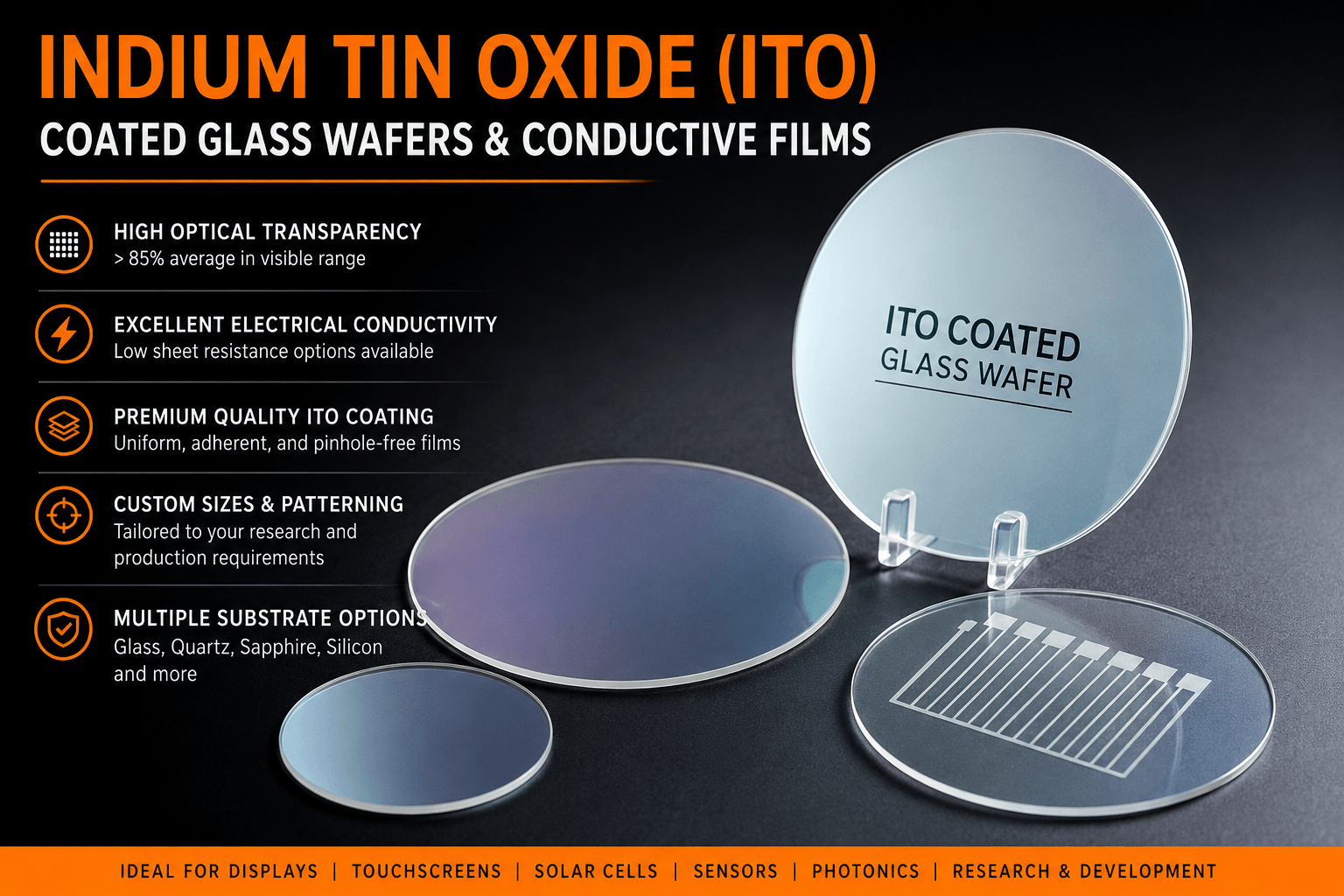
Indium Tin Oxide (ITO) is a transparent conductive oxide (TCO)
composed primarily of indium oxide (In2O3) with a small amount
of tin oxide (SnO2). This unique combination provides both
high electrical conductivity and
excellent optical transparency, making ITO one of the most widely
used thin-film materials
in modern electronics and optoelectronic devices.
ITO coatings are deposited onto
glass,
quartz,
sapphire,
silicon wafers,
and flexible polymers using techniques such as
sputtering
and electron beam evaporation. The resulting conductive surface allows
electrical current to flow while transmitting visible light with minimal loss.
Why Use ITO Coated Wafers?
ITO coated wafers provide an ideal platform for researchers developing
photodetectors,
MEMS devices,
solar cells,
transparent electronics, and
photonic devices.
Their combination of low electrical resistance, high optical transmission,
and excellent chemical stability makes them suitable for demanding
semiconductor and research applications.
| Property |
Benefit |
| High Optical Transparency |
Allows visible light transmission above 80–90%. |
| Excellent Electrical Conductivity |
Provides efficient transparent electrodes. |
| Low Sheet Resistance |
Improves display and sensor performance. |
| Chemical Stability |
Reliable in laboratory and industrial environments. |
| Photolithography Compatible |
Can be patterned using photolithography. |
| Multiple Substrates |
Available on glass, quartz, sapphire, silicon, PET, and PEN. |
Common Applications of ITO
Because of its unique optical and electrical properties, Indium Tin Oxide is
used throughout the semiconductor industry and university research
laboratories. Engineers rely on ITO whenever a material must conduct
electricity while remaining optically transparent.
Custom ITO Wafer Specifications
UniversityWafer supplies custom ITO coated substrates for research and
manufacturing. We can provide various coating thicknesses, sheet resistance
values, substrate materials, dimensions, and patterned electrode geometries.
Additional services include
wafer processing,
thin-film deposition,
polishing, dicing, cleaning, and custom fabrication.
| Customization |
Available Options |
| Substrate Material |
Glass, Quartz, Sapphire, Silicon, PET, PEN |
| ITO Thickness |
Custom thin-film deposition |
| Sheet Resistance |
Multiple resistance ranges |
| Patterning |
Custom electrode layouts |
| Wafer Size |
Research and production diameters |
| Surface Finish |
Single-side or double-side polished substrates |
Why Choose UniversityWafer?
For more than 30 years, UniversityWafer has supplied
silicon wafers,
SOI wafers,
III-V semiconductor substrates,
and specialty thin-film materials to universities, government laboratories,
and commercial manufacturers worldwide. Whether you require prototype
quantities or production volumes of ITO coated substrates, we can provide
materials manufactured to your exact specifications with fast turnaround.
Related Pages
