
What Is TEOS Oxide?
TEOS oxide is a silicon dioxide (SiO2) thin film deposited using tetraethyl orthosilicate (TEOS) as a silicon precursor. TEOS-based processes are widely used in semiconductor manufacturing and research because they can produce uniform oxide films with good conformality across patterned wafer surfaces.
TEOS oxide can be deposited using several chemical vapor deposition techniques, including low-pressure chemical vapor deposition (LPCVD) and plasma-enhanced chemical vapor deposition (PECVD). The appropriate process depends on factors such as allowable processing temperature, desired film properties, wafer structure, and device requirements.
Why Use TEOS for Silicon Dioxide Deposition?
Silicon dioxide is one of the most important dielectric materials used in semiconductor processing. TEOS provides an alternative oxide deposition method when a deposited SiO2 layer is required rather than an oxide produced by directly oxidizing the underlying silicon.
A major advantage of TEOS-derived oxide is its ability to coat complex surface features. This makes the process useful for wafers containing patterned structures, trenches, steps, and other topography where film uniformity and conformal coverage are important.
Key Advantages of TEOS Oxide
- Good conformality – TEOS processes can provide effective coverage over patterned and three-dimensional wafer structures.
- Uniform oxide films – Suitable deposition conditions can produce consistent SiO2 layers across the wafer.
- Electrical insulation – Silicon dioxide provides valuable dielectric properties for semiconductor and microelectronic devices.
- Process flexibility – TEOS can be incorporated into different CVD processes depending on temperature and film requirements.
- Broad research applications – Useful for semiconductor fabrication, MEMS, sensors, photonics, and thin-film experiments.
TEOS Oxide on Silicon Wafers
Silicon wafers with deposited TEOS oxide can be used as starting substrates for device fabrication and materials research. The oxide layer may function as an electrical insulator, passivation layer, masking material, sacrificial layer, or part of a more complex multilayer device structure.
Researchers can specify characteristics such as wafer diameter, silicon orientation, substrate type, oxide thickness, surface finish, and other processing requirements according to the intended experiment or fabrication process.
TEOS Oxide Applications
The combination of silicon dioxide's dielectric properties and the deposition capabilities of TEOS-based processes makes these films useful across many areas of semiconductor research and microfabrication.
- Semiconductor device fabrication
- MEMS and microsystems
- Interlayer dielectric structures
- Surface passivation
- Electrical isolation
- Thin-film research
- Sensor fabrication
- Microelectronics research
- Photonics and optical devices
- Wafer-level process development
Need TEOS Oxide Wafers for Your Research?
Get the TEOS oxide wafer specifications your project requires for semiconductor fabrication, MEMS, dielectric research, and thin-film processing.
Get Your TEOS Oxide Wafer Quote FAST!
Or,
Buy Wafers Online
and Start Researching Today!
TEOS Oxide Deposition Methods
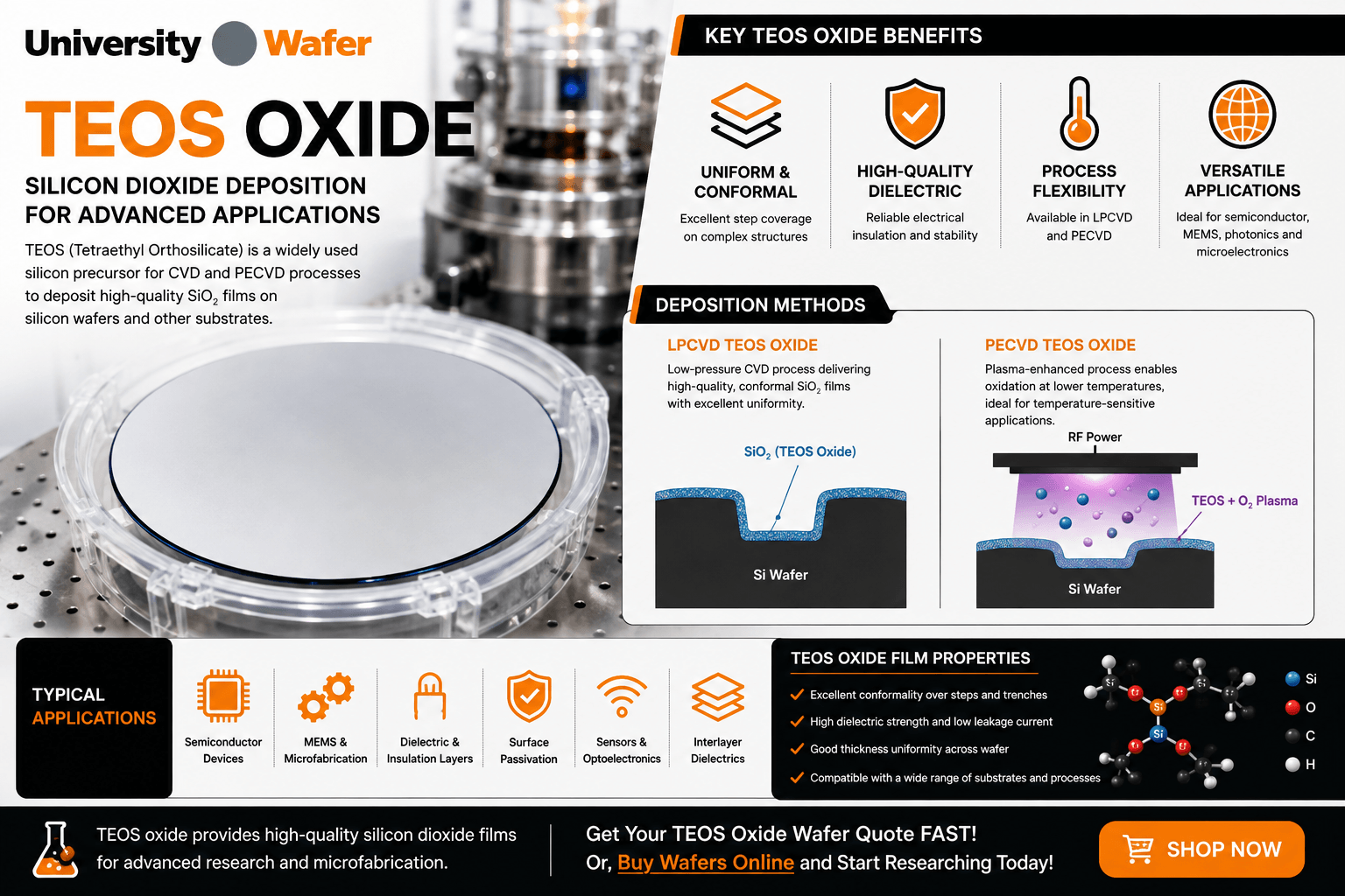
TEOS oxide films are commonly produced using chemical vapor deposition processes in which tetraethyl orthosilicate acts as the silicon-containing precursor. Process conditions can be adjusted to control properties such as film thickness, uniformity, density, stress, and conformality.
Depending on the application, researchers may use LPCVD TEOS or PECVD TEOS. These deposition methods provide different processing temperatures and film characteristics, allowing researchers to select an oxide process appropriate for their semiconductor or MEMS device.
LPCVD TEOS Oxide
Low-pressure chemical vapor deposition (LPCVD) can produce highly conformal TEOS-derived SiO2 films. This makes LPCVD useful when oxide coverage is required over patterned surfaces, steps, trenches, and other wafer topography.
Because LPCVD typically involves elevated processing temperatures, the thermal budget of the substrate and any previously fabricated structures should be considered when selecting the deposition process.
PECVD TEOS Oxide
Plasma-enhanced chemical vapor deposition (PECVD) uses plasma energy to assist chemical reactions, allowing silicon dioxide films to be deposited at lower substrate temperatures than many conventional thermal CVD processes.
Lower-temperature processing can be valuable for wafers containing temperature-sensitive materials or previously fabricated device layers. PECVD oxide is therefore widely investigated for passivation, dielectric layers, MEMS, sensors, and microelectronic structures.
TEOS Oxide vs. Thermal Oxide
Both TEOS oxide and thermal oxide provide silicon dioxide layers, but they are formed differently. Thermal oxidation consumes part of the underlying silicon substrate to create SiO2, while TEOS processes deposit an oxide film onto the wafer surface.
Because TEOS oxide is deposited rather than grown directly from silicon, it can be applied to a broader range of surfaces and existing device structures. Thermal oxide, however, is valued when a high-quality Si/SiO2 interface is particularly important.
Choosing an Oxide for Your Application
The appropriate oxide depends on the device architecture and fabrication process. Researchers should consider factors including oxide thickness, deposition temperature, conformality, electrical properties, surface topography, thermal budget, and subsequent processing steps.
- TEOS oxide: useful for deposited dielectric films and conformal coverage.
- Thermal oxide: useful when oxide can be grown directly from a silicon surface.
- PECVD oxide: useful when lower-temperature deposition is required.
- LPCVD TEOS: useful when conformal coverage across patterned structures is important.
TEOS Oxide for MEMS and Microfabrication
TEOS-derived silicon dioxide can play several roles during MEMS fabrication . Depending on the process, the oxide may serve as an insulating layer, masking layer, passivation film, structural component, or sacrificial material.
Its ability to coat patterned surfaces makes TEOS particularly useful when fabricating microscopic structures with steps and complex geometries. Controlled deposition can also support multilayer processes involving silicon, silicon nitride, metals, and other semiconductor materials.
TEOS Oxide Wafer Specifications
When selecting TEOS oxide wafers, researchers should consider both the deposited film and the underlying substrate. Important specifications may include:
- TEOS oxide thickness
- Film thickness uniformity
- Wafer diameter and thickness
- Silicon crystal orientation
- Substrate resistivity and doping
- Single-side or double-side oxide deposition
- Surface finish
- Film stress and density requirements
UniversityWafer supplies silicon wafers and processed substrates for semiconductor, MEMS, thin-film, and microfabrication research.