
What You Need to Know About Silicon Wafers for Electronics
- Silicon wafers are ultra-thin slices of semiconductor-grade silicon that serve as the foundation for electronic components
- Available in various diameters (150mm, 200mm, 300mm) with thicknesses ranging from 0.2-1.5mm
- Quality is determined by factors like purity (99.9999999% or higher), crystal structure, and surface finish
- Applications include computers, smartphones, solar panels, integrated circuits, and specialized electronics
- Selection should consider size, thickness, purity, surface finish quality, and compatibility with manufacturing processes
Get Your Quote FAST! Or, Buy Online and Start Your Research Today!
Introduction to Silicon Wafers in Electronics
Silicon wafers form the backbone of modern electronics, serving as the substrate upon which integrated circuits and semiconductor devices are built. These ultra-thin slices of semiconductor-grade silicon enable the creation of virtually all electronic devices we rely on today. Understanding the characteristics, manufacturing processes, and applications of silicon wafers is essential for anyone involved in electronics research, development, or production.

At University Wafer, we specialize in providing high-quality silicon wafers and other substrates for both research and production purposes. Silicon wafers are known for their exceptional purity, precise dimensions, and specific electrical properties, making them ideal for a wide range of electronic applications.
The right silicon wafer makes a big difference. The quality, specifications, and properties of the wafer directly impact the performance, reliability, and efficiency of the resulting electronic devices. In this guide, we'll explore silicon wafers, from their basic properties to how to choose the right ones for specific electronic applications.
Understanding Silicon Wafer Fundamentals
What Are Silicon Wafers?
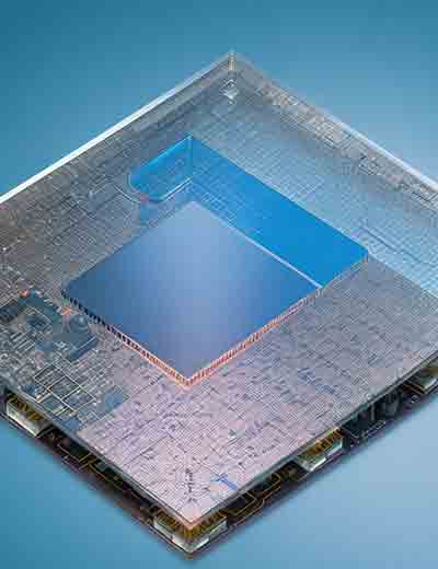
Silicon wafers are thin, circular discs cut from ingots of crystalline silicon. These wafers serve as the foundation for the fabrication of semiconductor devices and integrated circuits. The manufacturing process begins with the growth of a silicon crystal, typically using the Czochralski method, which results in a cylindrical ingot of highly pure silicon. This method involves melting polycrystalline silicon in a quartz crucible at temperatures exceeding 1,400°C and slowly drawing a seed crystal to form a single-crystal ingot with precisely controlled electrical and mechanical properties.

The silicon boule is then sliced into thin wafers, which undergo a series of processing steps including edge grinding, lapping, etching, polishing, and cleaning. These processes ensure that the wafers meet the strict requirements for flatness, thickness uniformity, and surface quality needed for semiconductor fabrication. Modern slicing techniques use diamond-wire saws that can cut wafers as thin as 100 micrometers while maintaining precise dimensions. The multi-stage polishing process achieves surface roughness values of less than 1 nanometer, essential for high-resolution photolithography in advanced semiconductor manufacturing.
Silicon Wafer Properties and Specifications
Silicon wafers are characterized by several key specifications:
- Diameter: Standard wafer diameters include 150mm (6 inches), 200mm (8 inches), and 300mm (12 inches), with the industry trending toward larger sizes for improved efficiency. Leading manufacturers are currently developing 450mm (18-inch) wafers to further increase production economies of scale.
- Thickness: Wafer thickness typically ranges from 0.2mm to 1.5mm, with the specific thickness dependent on the wafer diameter and intended application. The thickness-to-diameter ratio must be carefully controlled to prevent warping while maintaining mechanical stability during high-temperature processing steps.
- Crystal Orientation: Silicon wafers feature specific crystal orientations, commonly designated as (100), (111), or (110), which influence the electrical and mechanical properties of the wafer. The (100) orientation is most common in CMOS technology due to its favorable interface properties with silicon dioxide, while (111) orientation offers advantages for certain power devices.
- Dopant Type and Concentration: Wafers may be doped with elements like boron (p-type) or phosphorus (n-type) to modify their electrical conductivity. Dopant concentrations typically range from 10^14 to 10^19 atoms per cubic centimeter, allowing precise control of resistivity values.
- Resistivity: This measures the wafer's resistance to electrical current flow, typically ranging from 0.001 to 10,000 ohm-cm. High-precision four-point probe measurements ensure uniform resistivity across the entire wafer surface, critical for consistent device performance.
300mm (12-inch) silicon wafers have become increasingly common in high-volume manufacturing due to their ability to produce more chips per wafer, though smaller diameters remain important for specialized applications and research. The move to larger wafer sizes has historically reduced costs by about 30% per chip area, driving the semiconductor industry to pursue larger diameter substrates despite the significant engineering challenges involved.
Types of Silicon Wafers for Electronics Applications
Silicon Wafer Grades and Classifications
Silicon wafers are classified into different grades based on their quality and intended applications. Understanding these classifications is crucial for selecting the appropriate wafer for specific electronic applications. The semiconductor industry has established standardized specifications through organizations like SEMI (Semiconductor Equipment and Materials International) to ensure consistency across global supply chains.
Silicon wafer grades typically include:
- Prime Grade: The highest quality wafers with minimal defects, used for advanced semiconductor manufacturing. These wafers comply with the strictest specifications for particle contamination (typically fewer than 10 particles larger than 0.3μm per wafer), metallurgical defects (less than 0.1/cm²), and surface micro-roughness (below 0.5nm RMS). Prime grade wafers cost more but give better device yields.
- Test Grade: Slightly lower quality than prime grade, suitable for process development and testing. These wafers may have minor edge chips, slightly higher defect densities, or small deviations from flatness specifications, but remain suitable for most development work where ultimate yield is not critical.
- Reclaimed Wafers: Previously used wafers that have been cleaned and repolished, offering a cost-effective alternative for less demanding applications. The reclamation process typically removes 5-10μm of surface material, eliminating previous device structures while preserving the wafer's mechanical integrity. These wafers are widely used for equipment calibration and non-critical process steps.
- Monitor Wafers: Used for monitoring and calibrating equipment in semiconductor fabrication facilities. These wafers often incorporate specific test structures or materials to validate process parameters such as film thickness uniformity, etch rates, or implant doses without using expensive device wafers.
Each grade offers different levels of quality, specifications, and price points, allowing engineers and researchers to select the most appropriate option for their specific requirements. The price difference between grades can be substantial, with prime wafers often costing 2-5 times more than reclaimed wafers of the same diameter, making grade selection an important economic consideration in both research and production environments.
Specialized Silicon Wafer Types
Beyond the standard classifications, there are several specialized types of silicon wafers designed for specific applications:
- Ultra-Thin Wafers: With thicknesses down to a few microns, these wafers are essential for applications requiring minimal thickness, such as flexible electronics and advanced packaging technologies. Manufacturing these wafers requires specialized handling equipment and temporary bonding techniques to prevent breakage during processing. The increasing demand for thinner mobile devices and 3D-stacked integrated circuits has driven significant advances in ultra-thin wafer technology.
- High-Resistivity Wafers: Featuring resistivity values exceeding 1,000 ohm-cm, these wafers are ideal for RF and microwave applications where signal loss must be minimized. The extremely low concentrations of electrically active impurities (typically below 10^13 atoms/cm³) in these wafers require specialized purification techniques and careful contamination control throughout the manufacturing process.
At University Wafer, we offer a wide range of specialized silicon wafers, including ultra-thinned wafers and high certified bulk lifetime silicon wafers, to meet the diverse needs of our customers in the electronics industry. Our inventory includes wafers with specialized dopant profiles, custom orientations, and special surface treatments designed for new applications in quantum computing, photonics, and bioelectronics.
Selecting the Best Silicon Wafers for Specific Electronic Applications
Factors to Consider When Choosing Silicon Wafers
Selecting the right silicon wafer for a specific electronic application requires careful consideration of several key factors:
Different applications have unique requirements for electrical properties, mechanical strength, and thermal characteristics. For instance, high-frequency RF devices work better with high-resistivity substrates that minimize signal losses, while power electronics need wafers with excellent thermal conductivity to dissipate heat efficiently. Understanding what performance factors matter most for your application is the first step in wafer selection.
The specific semiconductor technology being implemented (CMOS, bipolar, MEMS, etc.) will influence wafer selection. Advanced CMOS nodes below 10nm typically need wafers with extremely tight flatness specifications (total thickness variation <1μm) and near-perfect crystal structure to ensure reliable lithography at these dimensions. MEMS applications often need thicker wafers with specific crystal orientations to enable anisotropic etching techniques.
The wafer must work with your intended fabrication processes, including lithography, etching, deposition, and thermal treatments. Process temperatures, chemical exposures, and mechanical stresses must all be considered when selecting wafer specifications. For example, wafers that will undergo high-temperature processing (>1000°C) require higher oxygen content to prevent defect formation during thermal cycling.
Budget constraints may require trade-offs between wafer specifications and cost. While prime-grade 300mm wafers offer the highest quality, they can cost several hundred dollars each, making them impractical for early-stage research or low-volume production. Reclaimed wafers or smaller diameters may provide acceptable performance at much lower cost for many applications.
Silicon Wafers for Integrated Circuits and Microprocessors
Integrated circuits and microprocessors form the core of modern computing devices, from smartphones to supercomputers. These applications typically require silicon wafers with the following characteristics:
Modern microprocessor fabrication requires silicon with 9N purity (99.9999999% pure) or better, as even tiny amounts of certain metallic contaminants can significantly impact device performance and reliability. Advanced purification techniques including zone refining and floating-zone crystallization are used to achieve these extraordinary purity levels.
Silicon chips are the end products created from silicon wafers through complex fabrication processes. The quality of the initial wafer directly impacts the performance, yield, and reliability of these chips. Modern semiconductor fabrication involves hundreds of precisely controlled process steps including photolithography, ion implantation, chemical vapor deposition, and plasma etching, with the entire manufacturing sequence taking 10-12 weeks to complete for advanced logic devices. A single defect in the silicon substrate can affect these processes, potentially making entire chips or regions of the wafer unusable.
Advanced Silicon Wafer Technologies for Cutting-Edge Electronics
Silicon-on-Insulator (SOI) Wafers
Silicon-on-Insulator (SOI) technology represents a significant advancement in silicon wafer technology, offering several advantages for electronic applications:
The insulating layer minimizes capacitive coupling to the substrate, enabling faster device operation. This reduction in parasitic capacitance can improve circuit switching speeds by 20-35% compared to bulk silicon implementations, particularly helpful for high-frequency applications above 5GHz. The buried oxide layer (typically 145-200nm thick) effectively isolates the active device layer from the substrate, eliminating junction capacitances that limit performance in conventional designs.
Devices are electrically isolated from each other, reducing cross-talk and improving performance. Complete dielectric isolation eliminates the need for complex well structures and guard rings typically required in bulk CMOS, simplifying design and reducing chip area by up to 15%. This isolation also provides natural immunity to latch-up problems that can affect conventional CMOS circuits under certain operating conditions.
SOI devices typically operate at lower power levels due to reduced leakage currents. The elimination of reverse-biased junction leakage paths can reduce standby power consumption by 50% or more compared to equivalent bulk silicon designs, making SOI particularly valuable for battery-powered and energy-efficient applications. Fully-depleted SOI (FD-SOI) technology further enhances these benefits by enabling operation at lower supply voltages.
Compound Semiconductor on Silicon
While pure silicon wafers dominate the semiconductor industry, there is growing interest in integrating compound semiconductors with silicon substrates:
Gallium Nitride (GaN) on Silicon is a prime example of this approach, combining the superior electronic properties of GaN (high electron mobility, wide bandgap) with the cost advantages and established manufacturing infrastructure of silicon wafers. These hybrid substrates offer:
Advanced epitaxial growth techniques using metal-organic chemical vapor deposition (MOCVD) can achieve GaN layers with thickness uniformity better than ±2% across 200mm silicon substrates. This uniformity is critical for maintaining consistent device characteristics and maximizing manufacturing yield. Buffer layer architectures with carefully engineered strain compensation prevent wafer bowing despite the significant lattice mismatch between GaN and silicon.
The wide bandgap of GaN (3.4eV compared to silicon's 1.1eV) results in much lower leakage currents at high temperatures and high electric fields. GaN-on-silicon power devices can maintain leakage currents below 1μA/mm² at blocking voltages exceeding 600V, enabling high-efficiency power conversion systems with reduced cooling requirements and smaller form factors.
Manufacturing Considerations for High-Quality Silicon Wafers
Cleanroom Requirements and Contamination Control
The manufacturing of high-quality silicon wafers demands strict cleanroom environments and contamination control measures:
Silicon wafer production typically occurs in Class 10 (ISO 4) or cleaner environments, where the number of particles per cubic foot is strictly limited. These facilities maintain fewer than 10 particles larger than 0.5μm per cubic foot of air, requiring sophisticated air filtration systems with multiple HEPA and ULPA filter stages. The cleanroom design incorporates laminar airflow patterns, pressure gradients between zones, and specialized construction materials to minimize particle generation and accumulation.
Potential sources of contamination include airborne particles, process chemicals, equipment surfaces, and human operators. Molecular contamination from volatile organic compounds (VOCs), acids, bases, and dopants must be controlled to parts-per-trillion levels for advanced wafer manufacturing. Specialized monitoring equipment including laser particle counters, residual gas analyzers, and surface analysis tools continuously verify contamination levels throughout the production environment.
Quality Control and Testing Methods
Ensuring the quality of silicon wafers involves a comprehensive suite of testing and characterization methods:
Non-contact metrology systems employing capacitive sensors or interferometric techniques can measure thickness variations with nanometer-scale resolution across the entire wafer surface. Total thickness variation (TTV), bow, warp, and site flatness are critical parameters measured during final inspection, with sophisticated data analysis software generating detailed topographic maps to verify compliance with specifications.
Automated systems detect and classify surface defects, including particles, scratches, and crystal imperfections. Laser scanning systems can detect particles as small as 30nm on polished wafer surfaces, with pattern recognition algorithms classifying defects by type, size, and potential impact on device yield. These systems can inspect an entire 300mm wafer in less than a minute, providing comprehensive defect maps that guide acceptance decisions and process improvement efforts.
Conclusion
Silicon wafers remain the foundation of modern electronics, enabling the incredible technological advances we've seen in computing, communications, and countless other fields. From simple diodes to complex microprocessors with billions of transistors, silicon wafers provide the perfect substrate for building the devices that power our digital world.
As technology continues to advance, the demands on silicon wafer quality, purity, and performance will only increase. Understanding the fundamentals of silicon wafer technology and the factors that determine which wafers are best for specific applications is essential for engineers, researchers, and professionals working in electronics-related fields.
Whether you're developing cutting-edge quantum computing components or manufacturing power electronics for electric vehicles, choosing the right silicon wafer is a critical first step toward success. By considering factors like wafer grade, diameter, thickness, resistivity, and surface quality, you can ensure that your electronic devices are built on a solid foundation.