
Indium Arsenide (InAs) Wafers & Substrates
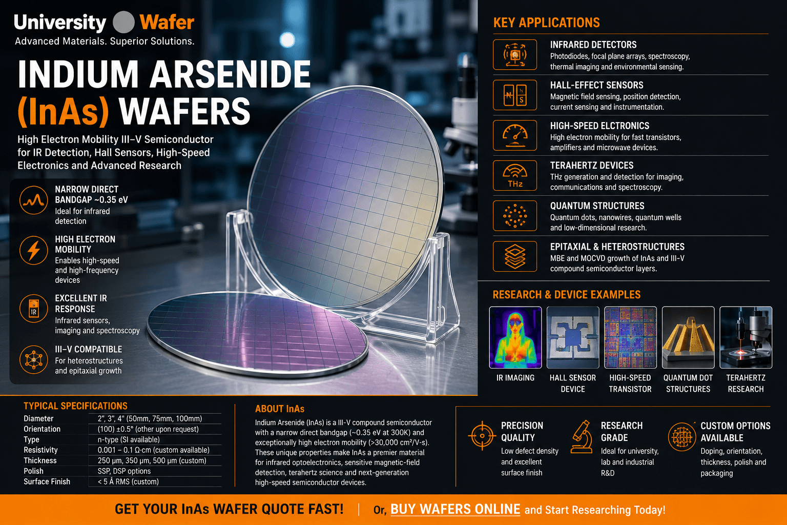
Indium Arsenide (InAs) is a III-V compound semiconductor composed of indium and arsenic. Its narrow direct bandgap and exceptionally high electron mobility make InAs an important material for infrared optoelectronics, high-speed electronics, magnetic-field sensing, and advanced semiconductor research.
UniversityWafer supplies InAs wafers and substrates for universities, research laboratories, semiconductor developers, and industrial R&D. InAs substrates can be used for device fabrication, thin-film studies, epitaxial growth, material characterization, and experimental III-V semiconductor structures.
Why Use InAs Wafers?
InAs has a direct bandgap of approximately 0.35 eV at room temperature. This narrow bandgap provides sensitivity to infrared wavelengths, while its high electron mobility makes the material attractive for devices requiring rapid carrier transport.
Important properties of Indium Arsenide include:
- Narrow direct bandgap: Suitable for infrared detection and optoelectronic research.
- High electron mobility: Valuable for high-speed and high-frequency electronic devices.
- Infrared response: Useful for detectors, sensors, spectroscopy, and imaging research.
- III-V compatibility: Suitable for epitaxial heterostructures involving other compound semiconductors.
- Small effective electron mass: Important for advanced transport, quantum, and low-dimensional semiconductor studies.
InAs for Infrared Detectors
InAs infrared detectors are studied for applications requiring sensitivity beyond the visible spectrum. InAs-based photodetectors can be used in infrared spectroscopy, thermal sensing, scientific instrumentation, environmental monitoring, and other optical detection systems.
Researchers developing infrared technologies may also investigate Indium Antimonide (InSb) wafers and Gallium Antimonide (GaSb) wafers depending on the desired wavelength range and device structure.
Hall-Effect & Magnetic Sensors
The high electron mobility of InAs makes it useful for Hall-effect sensors designed to detect magnetic fields. Hall devices measure the voltage generated when charge carriers moving through a semiconductor are exposed to a magnetic field.
InAs-based Hall sensors are researched for magnetic-field measurement, position sensing, current sensing, scientific instrumentation, and other applications where sensitive electronic detection is required.
High-Speed Electronics
Fast electron transport makes InAs an important research material for high-speed and high-frequency semiconductor devices. InAs and InAs-containing heterostructures are investigated for advanced transistors, electronic transport structures, and devices where carrier mobility can influence switching speed and frequency performance.
Other III-V materials, including Gallium Arsenide (GaAs), are also widely used for high-frequency and optoelectronic semiconductor research.
Quantum & Nanostructure Research
Indium Arsenide is widely studied in quantum dots, nanowires, low-dimensional structures, and semiconductor heterostructures. Its electronic properties allow researchers to investigate carrier confinement, quantum transport, nanoscale electronics, and other emerging semiconductor technologies.
Epitaxial Growth on InAs
InAs substrates can provide a crystalline foundation for growing III-V semiconductor layers and heterostructures. Techniques such as Molecular Beam Epitaxy (MBE) can be used to precisely control layer composition, thickness, doping, and interfaces during advanced material research.
Selecting an InAs Substrate
The appropriate Indium Arsenide wafer depends on the intended experiment or fabrication process. Researchers should consider specifications such as wafer diameter, crystal orientation, thickness, conductivity type, carrier concentration, surface finish, and polishing requirements.
Selecting the correct substrate specifications is particularly important for epitaxial growth and device fabrication, where crystal orientation and surface quality can affect subsequent semiconductor layers and device performance.
Get Your Indium Arsenide (InAs) Wafer Quote FAST! Or, Buy Wafers Online and Start Researching Today!
Indium Arsenide Applications
Indium Arsenide (InAs) wafers are used in advanced electronic, infrared, photonic, and quantum research because of their narrow direct bandgap and exceptionally high electron mobility. These properties make InAs particularly valuable when conventional silicon cannot provide the required infrared response or carrier transport performance.
Infrared Photodetectors & Imaging
InAs is an important material for infrared photodetectors. Its narrow bandgap enables detection of infrared radiation, making InAs-based structures useful for spectroscopy, thermal sensing, imaging, scientific instrumentation, and environmental monitoring.
Common infrared research applications include:
- Infrared photodiodes
- Optical and thermal sensors
- Infrared spectroscopy
- Gas and chemical detection
- Scientific imaging systems
- Environmental sensing
High-Speed Transistors
The high electron mobility of InAs makes the material attractive for high-speed and high-frequency transistor research. Rapid electron transport can support semiconductor structures designed for fast switching and operation at high frequencies.
InAs may be incorporated into heterostructures and nanoscale devices where researchers are investigating next-generation transistors, high-frequency electronics, and low-power semiconductor technologies.
Hall-Effect Sensors
InAs Hall-effect devices can provide high sensitivity to magnetic fields because of the material's favorable carrier transport properties. These sensors can be investigated for position detection, current measurement, magnetic-field characterization, and laboratory instrumentation.
Terahertz Research
InAs is also studied for terahertz (THz) generation and detection. Its high carrier mobility and fast electronic response make InAs-based structures interesting for experiments involving frequencies between the microwave and infrared regions of the electromagnetic spectrum.
Potential research areas include THz spectroscopy, imaging, communications, material characterization, and semiconductor-based THz emitters and detectors.
Quantum Dots & Nanostructures
Indium Arsenide is widely investigated for quantum dots, nanowires, quantum wells, and other low-dimensional semiconductor structures. These structures allow researchers to study quantum confinement and precisely engineered electronic states at extremely small dimensions.
InAs quantum structures can be combined with other III-V materials, including Gallium Arsenide (GaAs), to create semiconductor heterostructures for photonic and quantum-device research.
InAs/GaSb Heterostructures
InAs can be combined with Gallium Antimonide (GaSb) to form specialized III-V heterostructures. InAs/GaSb material systems are studied for infrared optoelectronics, quantum wells, superlattices, and advanced electronic devices.
These structures allow researchers to engineer electronic and optical properties by controlling semiconductor composition, layer thickness, and interfaces.
InAs Epitaxial Growth
High-quality InAs substrates provide a crystalline platform for III-V epitaxial growth. Researchers can use processes such as Molecular Beam Epitaxy (MBE) to grow precisely controlled semiconductor layers, quantum structures, and heterostructures.
Metalorganic Chemical Vapor Deposition (MOCVD) is another important technique used for the epitaxial growth of III-V semiconductor materials.
InAs Wafer Specifications
Choosing the correct InAs substrate specifications is important for successful device fabrication and epitaxial research. Depending on the application, researchers may need to consider:
- Wafer diameter
- Crystal orientation
- Wafer thickness
- n-type or semi-insulating characteristics
- Carrier concentration
- Doping requirements
- Single-side or double-side polishing
- Surface roughness and finish
InAs for Advanced Semiconductor Research
From infrared detectors and Hall sensors to high-speed electronics and quantum nanostructures, Indium Arsenide wafers provide researchers with a versatile platform for investigating semiconductor technologies that require high carrier mobility, infrared sensitivity, and compatibility with III-V heterostructures.