
What Is Aluminum Phosphide (AlP)?
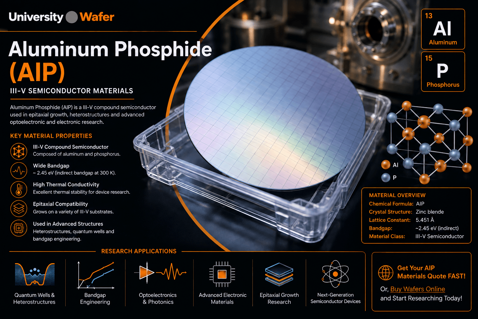
Aluminum Phosphide (AlP) is a III-V compound semiconductor composed of aluminum and phosphorus. In semiconductor research, AlP is of interest for studying wide-bandgap materials, epitaxial layers, semiconductor alloys, and heterostructures.
AlP can be incorporated into engineered III-V material systems where researchers need precise control over composition, crystal structure, and electronic properties. Rather than being limited to bulk material applications, AlP is particularly relevant to epitaxial semiconductor research and the development of advanced multilayer structures.
AlP as a III-V Semiconductor
Aluminum Phosphide belongs to the III-V semiconductor family, which combines elements from groups III and V of the periodic table. This family includes technologically important materials such as GaAs, GaP, InP, AlAs, and related ternary and quaternary semiconductor alloys.
III-V materials are widely investigated because their electronic and optical properties can be engineered by changing material composition and layer structure. AlP can therefore play a role in research involving bandgap engineering, lattice-matched structures, strained layers, and semiconductor heterojunctions.
Aluminum Phosphide Material Properties
The properties of AlP make it useful for specialized compound-semiconductor research. Important characteristics researchers may consider include:
- III-V compound semiconductor – Formed from aluminum and phosphorus.
- Wide bandgap – Relevant to semiconductor structures requiring larger energy-band separation.
- Crystalline material – Can participate in epitaxial structures with compatible semiconductor materials.
- Alloy compatibility – Useful in engineered III-V alloys and multilayer semiconductor systems.
- Band structure engineering – Composition can be incorporated into structures designed to control carrier confinement and electronic behavior.
AlP for Epitaxial Growth
Epitaxial growth allows researchers to deposit crystalline semiconductor layers on a suitable substrate while maintaining a controlled relationship with the underlying crystal lattice. AlP-containing layers may be investigated using advanced growth methods such as Molecular Beam Epitaxy (MBE) and other compound-semiconductor epitaxy techniques.
Precise epitaxial control enables researchers to create thin layers and multilayer structures in which composition, thickness, interfaces, and strain can be engineered for specific experimental requirements.
AlP Semiconductor Heterostructures
A major area of interest for AlP is the development of semiconductor heterostructures. A heterostructure combines two or more semiconductor materials with different electronic properties to produce engineered interfaces.
These structures can be designed to manipulate carrier transport, optical response, band alignment, and quantum confinement. AlP-containing layers may therefore be investigated as part of more complex III-V material systems rather than as an isolated semiconductor.
AlP and III-V Semiconductor Alloys
Semiconductor researchers can combine III-V compounds to form alloys with properties between those of the constituent materials. Aluminum-containing phosphide systems can provide additional flexibility when designing bandgaps, lattice parameters, and heterostructure interfaces.
This type of materials engineering is important for experimental structures used in optoelectronics, photonics, quantum research, and advanced semiconductor devices.
Applications of Aluminum Phosphide in Semiconductor Research
AlP and AlP-containing semiconductor structures may be relevant to research involving:
- III-V semiconductor heterostructures
- Wide-bandgap semiconductor research
- Epitaxial thin-film growth
- Bandgap engineering
- Quantum wells and multilayer structures
- Optoelectronic materials
- Photonics research
- Compound-semiconductor alloys
- Advanced electronic materials
- Next-generation semiconductor device research
Get Your AlP Semiconductor Materials Quote FAST! Or, Buy Wafers Online and Start Researching Today!
AlP for Bandgap Engineering
Aluminum Phosphide (AlP) is useful in III-V semiconductor research where the electronic properties of a multilayer structure must be carefully engineered. By incorporating AlP or AlP-containing alloys into epitaxial structures, researchers can investigate how composition influences band alignment, carrier confinement, optical response, and interface behavior.
Bandgap engineering is particularly important in heterostructures, where different semiconductor layers are combined to control the movement of electrons and holes. These principles are used extensively in advanced electronics, photonics, and quantum-device research.
AlP in Quantum Wells and Multilayer Structures
Precisely controlled semiconductor layers can create quantum wells and other quantum-confined structures. In these systems, a thin semiconductor layer is positioned between materials with different energy-band characteristics, restricting carrier motion at very small dimensions.
Advanced epitaxial techniques such as Molecular Beam Epitaxy (MBE) can provide the layer-thickness and interface control required to investigate these complex III-V structures.
Importance of Lattice Matching
Lattice matching is an important consideration when designing AlP-containing epitaxial structures. Differences between the lattice parameters of a deposited semiconductor and its underlying substrate can introduce strain into the growing crystal.
Researchers therefore consider substrate composition, crystal orientation, layer thickness, thermal behavior, and lattice compatibility when designing epitaxial experiments. Controlled strain can sometimes be intentionally incorporated into semiconductor structures, while excessive mismatch may contribute to crystalline defects and dislocations.
Choosing a Substrate for AlP Research
Substrate selection can strongly influence the quality of an epitaxial semiconductor structure. Researchers working with AlP and related III-V materials may evaluate several wafer characteristics before beginning deposition.
- Substrate material and composition
- Crystal orientation
- Lattice compatibility
- Wafer diameter and thickness
- Surface polish and roughness
- Miscut or off-axis orientation
- Dopant type and concentration
- Electrical resistivity
- Surface cleanliness
- Crystal quality and defect density
AlP and Related III-V Materials
AlP is part of a much broader family of compound semiconductors. Combining different III-V materials allows researchers to create sophisticated structures with properties that cannot easily be obtained from a single bulk semiconductor.
Related materials used in compound-semiconductor research include gallium arsenide (GaAs) , indium arsenide (InAs) , indium phosphide (InP), gallium phosphide (GaP), AlGaAs, and other ternary or quaternary III-V alloys.
AlP for Photonics and Optoelectronics Research
Compound semiconductors are particularly important in photonics and optoelectronics because their electronic band structures can be engineered to control interactions between electrons and light.
AlP-containing material systems can be investigated as part of multilayer structures designed for optical and electronic research, including structures related to light emission, detection, carrier confinement, and wavelength-dependent semiconductor behavior.
Surface Quality for Epit axial Research
High-quality semiconductor surfaces are important for epitaxial growth because the deposited crystal begins forming directly at the substrate interface. Particles, contamination, surface damage, and unwanted oxide layers can influence nucleation and subsequent crystalline quality.
Appropriate wafer surface preparation and cleaning can therefore be an important step before thin-film deposition. The exact preparation method depends on the substrate and epitaxial material system being investigated.
AlP Research Applications
Aluminum Phosphide and related III-V material systems can support research into semiconductor structures where precise control of composition and interfaces is required. Potential research areas include:
- III-V epitaxial layers
- Semiconductor heterostructures
- Bandgap engineering
- Quantum-confined structures
- Wide-bandgap semiconductor research
- Photonics and optoelectronics
- Compound-semiconductor alloys
- Strained-layer structures
- Advanced electronic materials
- Semiconductor materials characterization
Choosing Semiconductor Materials for AlP Research
Successful AlP research requires careful consideration of the complete material system rather than the AlP layer alone. Researchers should evaluate lattice parameters, crystal orientation, band structure, thermal properties, layer thickness, substrate quality, and growth conditions when designing an experiment.
UniversityWafer supplies semiconductor wafers and substrates for epitaxial growth, III-V materials research, thin-film deposition, heterostructure development, and advanced semiconductor experiments.