
Key Takeaways
- Silicon wafers require edge-only handling to prevent contamination and damage to critical device areas
- Cleanroom environments with controlled temperature (18-25°C) and humidity (30-60%) are essential for maintaining wafer integrity
- Proper ESD protection including grounding equipment, ionizers, and anti-static measures is critical to prevent device damage
- Specialized storage containers made from non-contaminating materials protect wafers from moisture, light, and environmental contamination
- Different wafer types (CZ, FZ, SiC) require specific handling considerations based on their unique physical properties
- Proper inspection and quality control processes including visual, automated, and statistical methods ensure wafer integrity
- Comprehensive training programs and documented procedures are fundamental to consistent handling quality
- Industry standards from organizations like SEMI and ASTM provide frameworks for handling best practices
Get Your Quote FAST! Buy Online and Start Researching Today!
Introduction to Silicon Wafer Handling
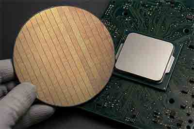
Silicon wafers are the foundation of modern electronics, serving as the substrate upon which integrated circuits and other semiconductor devices are built. These ultra-thin slices of semiconductor-grade silicon are delicate and require careful handling throughout their lifecycle. Improper handling can lead to contamination, scratches, cracks, or other damage that renders the wafers unusable for high-precision applications. Even microscopic defects can significantly impact device performance, reliability, and manufacturing yields, making proper handling protocols essential for successful semiconductor manufacturing.
At University Wafer, we understand the critical importance of proper wafer handling. Silicon wafers come in various diameters, from smaller 100mm (4-inch) wafers to larger 300mm (12-inch) and even 450mm wafers. Each size presents unique handling challenges, but the basic principles remain the same across all dimensions. The larger the wafer diameter, the more challenging the handling becomes due to increased surface area, weight, and chance of flexing or warping during manipulation.
The semiconductor industry's push toward smaller feature sizes and higher device densities makes proper handling practices more important than ever. Even tiny contaminants or minor physical damage can ruin an entire wafer's usability, resulting in significant financial losses and production delays. With feature sizes now in the nanometer range, particles that were once considered too small to matter can now cause major device failures. This article outlines the best practices for handling silicon wafers to ensure their integrity throughout manufacturing, processing, and research applications, providing complete guidance for maintaining wafer quality from initial production through final device fabrication.
Understanding Silicon Wafer Types and Properties
Before getting into handling practices, it's important to understand the different types of silicon wafers and their unique properties, as these characteristics influence specific handling requirements. The physical and chemical characteristics of different wafer types directly impact their sensitivity to handling stresses, contamination, and processing conditions, making this knowledge basic to proper handling protocols.
Czochralski (CZ) vs. Float Zone (FZ) Silicon Wafers

The two main methods for growing silicon ingots are the Czochralski (CZ) and Float Zone (FZ) processes. CZ and FZ silicon wafers differ in their oxygen content, crystal defects, and resistivity, which affects their applications and handling requirements. These basic differences come from their manufacturing processes and significantly impact their electrical, mechanical, and thermal properties.
CZ wafers contain higher oxygen concentrations (typically 10^17-10^18 atoms/cm³), making them stronger for thermal processing but potentially introducing unwanted impurities. The oxygen gets into the silicon during growth as the silicon melt contacts the quartz crucible. This oxygen provides helpful internal gettering effects that can trap metallic impurities away from device regions, but can also form thermal donors during certain temperature processes. CZ wafers generally offer greater mechanical strength and are less likely to be damaged during handling, making them the standard choice for most integrated circuit manufacturing.
FZ wafers, with their lower oxygen content (typically 10^15-10^16 atoms/cm³), offer higher resistivity and fewer crystal defects, making them ideal for high-performance devices but potentially more brittle during handling. The float zone process avoids crucible contact, resulting in extremely pure silicon with superior electrical characteristics. These wafers are preferred for power devices, radiation detectors, and other applications requiring high resistivity or minimal impurities. However, their lower oxygen content means they lack internal gettering capabilities and may require more careful handling to prevent mechanical damage.
Silicon Carbide and Other Specialty Wafers
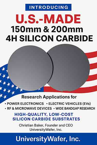
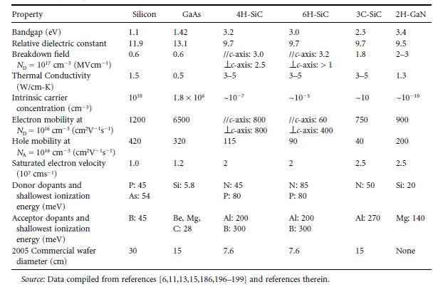
Silicon Carbide (SiC) wafers are increasingly important for high-power and high-temperature applications. These wafers offer superior thermal stability and breakdown voltage compared to standard silicon wafers but require specialized handling due to their hardness and brittleness. With a bandgap of approximately 3.2 eV (compared to silicon's 1.1 eV), SiC can operate at temperatures exceeding 600°C and withstand electric fields up to 10 times higher than silicon, making it ideal for power electronics, electric vehicles, and renewable energy applications.
SiC's extreme hardness (9.5 on the Mohs scale compared to silicon's 7) makes it resistant to scratching but also more difficult to process. Standard silicon processing equipment often requires modification or replacement when working with SiC. Additionally, SiC wafers typically have higher defect densities than silicon wafers, including micropipes, dislocations, and polytype inclusions, which can affect device performance and must be considered during handling and processing.
Other specialty wafers include those with thermal oxide layers or silicon nitride coatings, which serve specific purposes in semiconductor manufacturing but may have additional handling considerations to protect their surface properties. These engineered wafers feature precisely controlled films that provide electrical insulation, diffusion barriers, or surface passivation. Handling protocols must account for these films' specific chemical and mechanical sensitivities, often requiring more stringent contamination control and gentler physical handling than bare silicon wafers.
Physical Properties Affecting Handling
Silicon wafers possess several physical properties that directly impact handling requirements:
- Brittleness: Silicon is a brittle material that can crack or chip under stress. With a Mohs hardness of 7, silicon is harder than many metals but lacks ductility, making it susceptible to fracture when subjected to point loads or bending stresses. The crystalline structure of silicon follows defined cleavage planes, which can propagate cracks rapidly once initiated.
- Surface sensitivity: Even microscopic scratches can render areas of the wafer unusable. The highly polished surface of semiconductor-grade wafers typically has roughness measured in angstroms (Å), making even nanometer-scale damage significant. Surface defects can disrupt device patterning, cause electrical shorts or opens, and serve as nucleation sites for further defects during processing.
- Electrostatic sensitivity: Silicon wafers readily accumulate static charges that attract contaminants. The semiconductor properties of silicon make it particularly susceptible to electrostatic charging, with surface resistivity allowing charges to remain localized rather than dissipating quickly. These charges can exceed several thousand volts and cause both particle attraction and electrical damage to sensitive device structures.
- Thermal sensitivity: Rapid temperature changes can cause wafer warping or cracking due to thermal expansion. Silicon has a thermal expansion coefficient of approximately 2.6 × 10^-6 K^-1, which means temperature gradients across a wafer can induce significant stress. Larger diameter wafers are particularly susceptible to thermal warping due to their increased surface area relative to thickness.
- Chemical reactivity: Wafer surfaces can react with environmental contaminants. Clean silicon surfaces are highly reactive, readily forming native oxide layers when exposed to oxygen and adsorbing various organic and inorganic contaminants from the environment. These reactions can alter surface properties and affect subsequent processing steps.
Understanding these properties is crucial for implementing appropriate handling protocols that preserve wafer integrity throughout processing and transportation. The interaction between these physical characteristics and environmental factors determines the specific handling requirements for different wafer types and applications.
Cleanroom Requirements for Silicon Wafer Handling
The cornerstone of proper silicon wafer handling is the cleanroom environment. Cleanrooms provide controlled conditions that minimize particulate contamination, maintain appropriate temperature and humidity levels, and reduce the risk of electrostatic discharge. These specialized environments represent a substantial investment in infrastructure but are essential for maintaining wafer quality throughout processing.
Cleanroom Classification Standards
Cleanrooms are classified according to the number of particles of specific sizes permitted per cubic meter of air. For silicon wafer handling, particularly for advanced semiconductor manufacturing, ISO Class 5 (equivalent to Class 100) or cleaner environments are typically required. These environments limit particles of 0.5 μm and larger to fewer than 3,520 per cubic meter of air. To put this in perspective, ambient outdoor air typically contains millions of particles per cubic meter, making cleanrooms thousands of times cleaner than regular environments.
More critical processes, especially those involving the smallest feature sizes in cutting-edge semiconductor manufacturing, may require ISO Class 3 (Class 1) or cleaner environments. At University Wafer, we maintain appropriate cleanroom classifications for different wafer handling processes. The ISO 14644-1 standard defines these classifications and specifies the testing methodologies for verifying compliance, with regular monitoring required to maintain certification.
The classification system extends beyond particle counts to include other aspects of contamination control, such as airborne molecular contamination (AMC), which addresses gaseous contaminants that can react with wafer surfaces. Advanced facilities monitor and control specific gases like ammonia, acids, and volatile organics that can impact wafer processing even at part-per-billion concentrations.
Temperature and Humidity Control
Cleanrooms for silicon wafer handling must maintain precise temperature and humidity levels:
- Temperature: Typically maintained between 18-25°C (64-77°F), with variations limited to ±0.5°C per hour. This tight control prevents thermal stress on wafers and ensures consistent process conditions. Temperature stability is particularly critical during photolithography, where even minor variations can cause pattern misalignment due to thermal expansion or contraction of the wafer.
- Humidity: Usually controlled between 30-60% relative humidity, with 45-50% being optimal for balancing ESD protection and preventing moisture-related issues. Lower humidity increases static charge generation and retention, while higher humidity can promote chemical reactions on wafer surfaces and accelerate corrosion of equipment. Precise humidity control requires sophisticated HVAC systems with dedicated humidification and dehumidification capabilities.
Fluctuations outside these parameters can lead to wafer warping, enhanced electrostatic discharge risk, or accelerated chemical reactions on wafer surfaces. Modern cleanrooms employ redundant environmental monitoring systems that continuously track temperature and humidity, with automated controls to maintain stability and alert operators to any deviations from specifications.
Air Filtration and Flow
Proper air filtration and flow patterns are essential in cleanroom environments:
- HEPA (High-Efficiency Particulate Air) or ULPA (Ultra-Low Penetration Air) filtration systems capture particles as small as 0.1 μm with an efficiency of 99.99% or greater. These filtration systems represent multiple stages of progressively finer filtration, with pre-filters capturing larger particles to extend the life of the more expensive HEPA/ULPA filters.
- Laminar (unidirectional) airflow minimizes turbulence and particle movement across wafer surfaces. This flow pattern moves air in parallel streams from ceiling filters toward the floor, sweeping particles away from critical work areas. The airflow velocity is carefully controlled, typically between 0.3-0.5 m/s, to effectively remove particles without creating turbulence that could reintroduce contaminants into the work area.
- Air exchange rates typically range from 10-100 complete air changes per hour, depending on the cleanroom classification. Higher classifications require more frequent air changes to maintain cleanliness levels. This continuous air movement represents a significant energy investment but is essential for maintaining the ultra-clean environment required for wafer processing.
These systems work together to continuously remove airborne contaminants that could settle on wafer surfaces and compromise their integrity. The design of modern cleanrooms also incorporates pressure differentials between adjacent areas, with higher pressure in cleaner zones to prevent contaminant migration from less clean areas. This pressure cascade, combined with airlocks and gowning rooms, creates multiple barriers against environmental contamination.
Proper Handling Techniques for Silicon Wafers
The actual physical handling of silicon wafers requires specialized techniques and tools to prevent contamination and damage. The fundamental principle is to minimize contact with the wafer's surface while maintaining secure control. Proper handling techniques represent the front line of wafer protection, directly impacting yield and device performance.
Edge-Only Handling Principle
The most critical rule in silicon wafer handling is to touch only the edges of the wafer, never the polished surfaces. The edge exclusion zone (typically 2-5mm from the wafer's edge) is designated for handling, as devices are not fabricated in this area. This principle applies whether handling wafers manually or with automated equipment. The exclusion zone width varies with wafer diameter and application, with more advanced processes often specifying larger exclusion zones to accommodate the increased sensitivity of smaller device features.
When working with 150mm (6-inch) silicon wafers or larger sizes, edge-only handling becomes even more critical due to the increased surface area and potential for wafer bending or flexing during handling. Larger wafers have greater mass but proportionally less thickness relative to their diameter, making them more susceptible to mechanical stress during handling. The industry trend toward thinner wafers (often less than 775μm for 300mm wafers) further increases this challenge, requiring even more careful edge handling techniques.
The edge-only principle extends beyond manual handling to the design of automated equipment, wafer carriers, and process tools. Contact points are carefully engineered to touch only the wafer edge, with specialized materials chosen to minimize particle generation and contamination. Even robotic end effectors are designed with this principle in mind, using vacuum or edge-gripping mechanisms that preserve the integrity of the device area.
Specialized Handling Tools
Several specialized tools facilitate proper wafer handling:
- Vacuum wands: These tools use gentle suction to lift wafers by their edges or backsides. Modern vacuum wands feature precise control over suction force, soft contact materials, and ergonomic designs that minimize operator fatigue during extended use. Some advanced models include sensors that verify proper wafer engagement before lifting, preventing accidental drops.
- Teflon or ceramic tweezers: Non-metallic tweezers with flat, smooth tips designed specifically for wafer handling. These materials minimize particle generation and prevent scratching of the wafer surface. The tips are precisely manufactured with controlled dimensions and surface finish to provide secure gripping without excessive pressure that could damage the wafer edge.
- Wafer forks: Specialized tools that support wafers from beneath while minimizing contact area. These forks typically feature narrow contact points along the wafer edge, with materials chosen for cleanliness and minimal particle generation. Advanced designs incorporate static dissipative materials to prevent charge accumulation during handling.
- Automated handling systems: Robotic systems designed for precise, contamination-free wafer transfer. These systems range from simple transfer robots to complex integrated handling systems that move wafers between multiple process tools without human intervention. Modern systems incorporate vision systems for wafer alignment, force feedback for gentle handling, and sophisticated motion control for smooth acceleration and deceleration.
These tools should be regularly cleaned and inspected to ensure they don't introduce contamination or damage to the wafers. Cleaning protocols typically involve isopropyl alcohol or specialized cleanroom-compatible cleaning agents, with regular inspection under magnification to identify wear or damage that could compromise wafer integrity. Many facilities implement scheduled replacement of handling tools before they show signs of degradation.
Personal Protective Equipment
Proper personal protective equipment (PPE) is essential for wafer handling:
- Cleanroom gloves: Typically made from nitrile or latex, these should be powder-free and changed regularly. Glove selection considers factors like particle generation, chemical resistance, tactile sensitivity, and allergenic potential. Many facilities implement double-gloving protocols for critical operations, with the outer glove changed between handling different wafer lots to prevent cross-contamination.
- Cleanroom garments: Full coveralls, hoods, boot covers, and face masks that minimize particle shedding. These garments are manufactured from specialized fabrics that trap particles generated by the human body, preventing them from entering the cleanroom environment. The materials undergo stringent testing for particle shedding, durability, and comfort during extended wear. Garment designs eliminate potential particle traps like open pockets or exposed zippers.
- Anti-static wrist straps and footwear: These prevent electrostatic charge buildup that could damage wafers. Wrist straps typically connect to ground through a 1 megohm resistor that limits current for operator safety while effectively dissipating static charges. Footwear incorporates conductive elements that maintain electrical contact with grounded flooring, preventing charge accumulation during movement throughout the facility.
All PPE must be cleanroom-compatible and properly donned in the correct sequence through an established gowning procedure. Gowning procedures are carefully designed to minimize contamination, with specific sequences for donning different items and techniques for ensuring proper fit without generating particles. Many facilities use airlocks with tacky mats and air showers to remove loose particles before personnel enter the cleanroom proper.
Movement and Transfer Techniques
How wafers are moved and transferred is crucial to preventing damage:
- Maintain wafers in a horizontal position whenever possible to minimize stress and reduce the risk of dropping. When vertical orientation is necessary, specialized carriers with secure wafer retention features must be used to prevent slippage or contact between adjacent wafers.
- Avoid rapid movements that could create air currents and particle movement. Smooth, deliberate motions reduce turbulence around the wafer and minimize the risk of attracting airborne particles. Training typically emphasizes measured movements at consistent speeds rather than rapid acceleration or deceleration.
- Transfer wafers smoothly between surfaces, avoiding abrupt stops or starts that could cause wafers to slide or bounce. Proper transfer techniques include maintaining consistent height during horizontal transfers and using controlled descent rates when placing wafers onto surfaces.
- Keep handling time to a minimum, returning wafers to proper storage containers promptly to reduce exposure to potential contamination. Extended exposure to the cleanroom environment, even with excellent filtration, increases contamination risk. Many facilities implement protocols that specify maximum exposure times before wafers must be returned to sealed containers.
For 12-inch (300mm) silicon wafers, extra care is needed due to their larger diameter and increased susceptibility to warping during handling. These larger wafers represent significant value, with a single fully processed 300mm wafer potentially worth tens of thousands of dollars. Their increased diameter-to-thickness ratio makes them more flexible and susceptible to bending stresses during handling, requiring specialized equipment and handling protocols.
Electrostatic Discharge (ESD) Protection
Electrostatic discharge poses a significant threat to silicon wafers, particularly those with sensitive device structures. A single ESD event can damage or destroy devices on a wafer, making comprehensive ESD protection essential. Modern semiconductor devices, with gate oxides sometimes only a few atoms thick, can be damaged by static discharges well below the human perception threshold of approximately 3,000 volts.
Understanding ESD Risks
Silicon wafers can accumulate static charges through various mechanisms:
- Triboelectric charging (friction between materials) occurs when dissimilar materials contact and separate, transferring electrons between surfaces. The triboelectric series ranks materials by their tendency to gain or lose electrons, with materials far apart on the scale generating higher charges. Common cleanroom materials like plastics can generate significant charges when rubbed against other surfaces.
- Inductive charging (proximity to charged objects) happens when a charged object is brought near a conductive object without touching it, causing charge redistribution. This mechanism can charge wafers even without direct contact, making it particularly insidious in manufacturing environments.
- Conductive charging (direct contact with charged objects) transfers charges directly between objects. This can occur when wafers contact charged surfaces or handling equipment that hasn't been properly grounded.
These charges can reach several thousand volts and discharge rapidly when the wafer encounters a grounded object, potentially damaging sensitive structures on the wafer. The damage mechanisms include dielectric breakdown of thin gate oxides, junction damage from current surges, and metallization damage from localized heating during discharge events. Even if immediate catastrophic failure doesn't occur, ESD events can create latent defects that reduce device reliability and lifetime.
Grounding Equipment and Personnel
Proper grounding is the foundation of ESD protection:
- Personnel grounding: Achieved through wrist straps connected to ground points with 1MΩ resistors for safety. These resistors limit current flow to safe levels in case of accidental contact with live electrical circuits while still effectively dissipating static charges. Wrist straps should make firm contact with the skin and be tested daily using calibrated testers that verify both continuity and proper resistance.
- Equipment grounding: All processing and handling equipment must be properly grounded to a verified earth ground connection. This includes not only electrical equipment but also workbenches, storage racks, and transfer carts. Grounding connections should be regularly inspected for corrosion, loose connections, or damage that could compromise their effectiveness.
- Workstation grounding: Conductive or dissipative work surfaces connected to ground provide a controlled path for charge dissipation. These surfaces typically have resistance to ground in the range of 10^6 to 10^9 ohms, allowing charges to dissipate at a controlled rate without creating spark hazards. Regular cleaning with ESD-safe cleaners is essential to maintain proper surface resistivity.
Grounding systems should be regularly tested to ensure proper functionality, with records maintained of testing dates and results. Comprehensive testing programs include not only continuity checks but also resistance measurements and discharge time testing to verify that charges dissipate at appropriate rates. Many facilities implement automated monitoring systems that continuously verify the integrity of critical grounding connections.
Anti-Static Materials and Devices
Various anti-static materials and devices help prevent ESD damage:
- Ionizers: These devices neutralize static charges by releasing positive and negative ions into the air. Modern ionizers use corona discharge, alpha radiation, or other technologies to generate balanced ion streams that neutralize both positive and negative surface charges. Advanced models include feedback systems that monitor ion balance and output to maintain optimal performance. Strategic placement of ionizers throughout the handling area ensures comprehensive coverage of workspaces and transfer paths.
- Anti-static mats and flooring: These materials dissipate static charges safely through controlled conductivity. Floor materials typically incorporate conductive elements like carbon fibers or metal particles to provide paths for charge dissipation while maintaining durability under foot traffic. Mats often feature multiple layers with different electrical properties to optimize both charge dissipation and operator comfort.
- ESD-safe containers: Specialized containers that prevent charge buildup during wafer storage and transport. These containers use materials with controlled surface resistivity, often incorporating carbon or other conductive additives to provide charge dissipation without introducing contamination. Advanced designs include Faraday cage principles to shield contents from external electric fields.
- Humidity control: Maintaining relative humidity above 45% helps reduce static charge accumulation by creating a thin moisture layer on surfaces that enhances conductivity. This natural charge dissipation mechanism supplements other ESD controls but requires careful balancing to avoid moisture-related issues like corrosion or enhanced particle adhesion.
For handling high-mobility silicon wafers, additional ESD precautions may be necessary due to their increased sensitivity to electrical damage. These high-performance materials, with their enhanced carrier transport properties, can experience more severe effects from even minor ESD events, requiring comprehensive protection throughout handling and processing.
ESD Monitoring and Testing
Regular monitoring and testing of ESD protection measures ensure their effectiveness:
- Wrist strap testers verify proper grounding of personnel, checking both continuity and resistance values. Modern systems record test results electronically, ensuring compliance with testing schedules and maintaining documentation for quality assurance purposes. Some facilities implement continuous monitoring systems that verify wrist strap functionality throughout the work shift.
- Surface resistivity meters check work surfaces and flooring to verify appropriate charge dissipation properties. These measurements should be performed at multiple points across each surface, as localized damage or contamination can create areas with inadequate ESD protection. Testing schedules typically specify both routine verification and comprehensive mapping at longer intervals.
- Charge plate monitors measure ionizer effectiveness by determining how quickly a known charge is neutralized. These instruments provide quantitative data on neutralization times and ion balance, allowing optimization of ionizer placement and settings. Regular testing helps identify ionizers requiring maintenance or replacement before they fail to provide adequate protection.
- ESD event detectors identify potential problem areas by sensing discharge events in the handling environment. These devices can be fixed installations or portable units used for troubleshooting specific areas. Advanced systems provide data logging capabilities that help correlate ESD events with specific activities or equipment.
These testing procedures should be incorporated into standard operating procedures with clear documentation of results and corrective actions when necessary. A comprehensive ESD control program includes not only regular testing but also trend analysis to identify degrading performance before it reaches critical levels. Training programs should emphasize the importance of testing compliance and proper response to test failures.
Wafer Storage and Transportation
Proper storage and transportation are essential for maintaining wafer integrity between processing steps and during shipment to customers or other facilities. Even with perfect handling techniques, improper storage or transportation can introduce contamination or damage that compromises wafer quality.
Storage Container Requirements
Silicon wafers require specialized storage containers with specific properties:
- Material compatibility: Typically made from polypropylene, polycarbonate, or other non-contaminating materials that don't outgas harmful chemicals or shed particles. These materials undergo extensive testing for compatibility with wafers and cleanroom environments, including evaluation for particle generation, chemical emissions, and electrostatic properties. High-purity versions of these plastics are formulated specifically for semiconductor applications.
- Electrostatic properties: Containers should be either conductive or dissipative to prevent charge buildup. Conductive containers (typically carbon-filled) provide Faraday cage protection against external fields, while dissipative materials (often containing anti-static additives) prevent charge accumulation during handling. The choice between these options depends on the specific wafer type and sensitivity.
- Particle generation: Materials should have minimal particle shedding characteristics even after repeated use and cleaning. Container designs eliminate sharp corners, rough surfaces, and other features that could generate particles during wafer insertion or removal. Manufacturing processes for these containers include specialized molding techniques and post-production cleaning to minimize particulate contamination.
- Chemical resistance: Containers must resist degradation from cleaning agents and ambient chemicals commonly found in semiconductor environments. This resistance ensures long-term durability and prevents container degradation from becoming a contamination source. Materials are tested against a range of cleaning agents, solvents, and process chemicals to verify compatibility.
The most common storage options include:
- Cassettes: Slotted containers that hold multiple wafers vertically with minimal contact points. These provide efficient storage density while maintaining separation between wafers to prevent contact damage. Slot designs are precisely engineered to support wafers securely while minimizing contact area. Advanced designs incorporate features that prevent incorrect wafer insertion and provide visual verification of proper seating.
- Single-wafer containers: Individual containers for high-value or particularly sensitive wafers. These typically provide enhanced protection through cushioned supports and sealed environments. Some designs incorporate desiccants or inert gas purging for long-term storage of moisture-sensitive materials.
- Shipping boxes: Specialized containers designed to protect wafers during transportation. These incorporate multiple layers of protection, including shock-absorbing materials, moisture barriers, and tamper-evident seals. Designs vary based on shipping method (air, ground, sea) and distance, with international shipments requiring particularly robust protection.
Environmental Controls During Storage
The storage environment must be carefully controlled:
- Temperature: Typically maintained between 18-25°C (64-77°F) with minimal fluctuations to prevent thermal stress on wafers. Temperature stability is particularly important for wafers with deposited films that may have different thermal expansion coefficients than the silicon substrate. Storage facilities often implement redundant temperature control systems with continuous monitoring and alarm capabilities.
- Humidity: Usually kept between 30-60% relative humidity to balance ESD protection against moisture-related issues. Lower humidity increases static charge concerns, while higher humidity can promote chemical reactions or corrosion of metal films. Humidity control systems often include both humidification and dehumidification capabilities to maintain stable conditions regardless of external weather conditions.
- Air quality: Storage areas should have appropriate filtration, though not necessarily full cleanroom conditions. HEPA filtration is common in wafer storage areas, with air exchange rates designed to maintain appropriate cleanliness levels. Some facilities implement positive pressure differentials between storage areas and surrounding spaces to prevent contamination ingress.
- Light exposure: Protection from UV and other high-energy light sources that could affect photosensitive materials on wafer surfaces. This is particularly important for wafers with photoresist or other light-sensitive coatings. Storage areas often use amber lighting or light filters to minimize exposure to damaging wavelengths.
For long-term storage, additional considerations such as nitrogen purging or vacuum sealing may be implemented to prevent oxidation or contamination. These techniques are particularly important for wafers with exposed metal films or other materials susceptible to atmospheric degradation. Specialized cabinets with controlled atmospheres provide these capabilities while maintaining accessibility for inventory management.
Transportation Protocols
When transporting wafers between facilities, additional precautions are necessary:
- Shock absorption: Packaging must protect wafers from mechanical shocks during handling and shipping. Multiple layers of cushioning materials with different compression characteristics provide protection against both sharp impacts and prolonged vibration. Specialized foams, air cushions, and suspension systems are designed specifically for semiconductor shipping applications.
- Vibration damping: Materials that minimize vibration transfer to the wafers prevent micro-cracks and other damage during transportation. Vibration isolation systems may include elastomeric mounts, gas-filled cushions, or specialized foams with vibration-damping properties. Testing with accelerometers helps verify the effectiveness of these measures under real-world shipping conditions.
- Temperature stability: Insulated containers that prevent rapid temperature changes protect wafers from thermal stress during shipping through various climate zones. For particularly sensitive materials, active temperature control systems or phase-change materials may be incorporated to maintain stable temperatures throughout the shipping duration.
- Orientation control: Maintaining proper wafer orientation to prevent sliding or movement within containers is critical for preventing mechanical damage. Container designs incorporate features that lock wafers in position and provide visual indicators of proper orientation. Some shipping containers include orientation sensors that record potentially damaging position changes during transit.
- Contamination barriers: Multiple layers of protection against environmental contaminants ensure wafers arrive in clean condition. These may include sealed inner containers, moisture-proof barriers, and outer packaging designed to withstand handling without compromising internal cleanliness. Advanced packaging may incorporate desiccants, oxygen absorbers, or other active materials to maintain appropriate internal environments.
All transportation containers should be clearly labeled with handling instructions and fragility warnings to ensure proper care throughout the shipping process. Standardized symbols and handling instructions help ensure proper treatment regardless of language barriers or shipping provider. Many facilities implement tracking systems that monitor package location and environmental conditions throughout the shipping process.
Conclusion
Proper silicon wafer handling is fundamental to successful semiconductor manufacturing and research. The techniques and protocols outlined in this guide - from cleanroom requirements and edge-only handling to ESD protection and proper storage - work together to preserve wafer integrity throughout processing and transportation.
The key principles are straightforward: maintain clean environments, handle wafers only by their edges, protect against electrostatic discharge, and use appropriate storage containers. However, implementing these principles requires careful attention to detail, proper equipment, and comprehensive training for all personnel involved in wafer handling.
As the semiconductor industry continues advancing toward smaller feature sizes, larger wafer diameters, and new materials, handling requirements will become even more stringent. Organizations that invest in proper handling infrastructure and maintain rigorous protocols will achieve better yields, reduced defect rates, and improved device performance.
Success in wafer handling ultimately depends on understanding that these delicate substrates are the foundation of modern electronics. Every handling interaction - from initial production through final device fabrication - must prioritize wafer integrity to ensure the quality and reliability of the electronic devices that power our modern world.