
Understanding Silicon Doping and Carrier Mobility
Silicon doping is the controlled introduction of impurity atoms into crystalline silicon to modify its electrical properties. Pure intrinsic silicon contains relatively few free charge carriers at room temperature, so carefully selected dopants are added to increase the concentration of electrons or holes available for electrical conduction.
Although increasing the dopant concentration generally increases the number of available charge carriers, it can also decrease their carrier mobility. This occurs because ionized dopant atoms disturb the periodic crystal potential and increase scattering, making it more difficult for electrons and holes to move through the silicon lattice.
What Is Carrier Mobility?
Carrier mobility describes how readily electrons or holes move through a semiconductor when an electric field is applied. Mobility is commonly represented by the symbol μ and is typically expressed in cm2/V·s.
Higher mobility allows charge carriers to move more rapidly for a given electric field. Carrier mobility therefore plays an important role in semiconductor properties and can influence conductivity, resistivity, device speed, current capability, and overall electronic performance.
Electron vs. Hole Mobility in Silicon
Electrons and holes do not move through silicon with the same mobility. In lightly doped silicon near room temperature, electron mobility is generally higher than hole mobility because electrons and holes have different effective masses and interact differently with the silicon crystal lattice.
As doping concentration increases, the mobility of both carrier types generally decreases because of increased ionized-impurity scattering.
N-Type Silicon Doping
N-type silicon is produced by introducing donor impurities that provide additional electrons. Common donor dopants for silicon include phosphorus, arsenic, and antimony.
In n-type material, electrons are the majority carriers while holes are the minority carriers. Increasing donor concentration increases the electron concentration, but at sufficiently high doping levels the additional ionized impurities also increase scattering and reduce electron mobility.
P-Type Silicon Doping
P-type silicon is created using acceptor dopants that produce holes as the majority carriers. Boron is one of the most commonly used p-type dopants in silicon semiconductor processing.
As acceptor concentration increases, the hole concentration rises while hole mobility generally decreases due to stronger interactions with ionized impurities within the crystal.
Why Higher Doping Reduces Mobility
At lower dopant concentrations, carrier mobility is strongly influenced by interactions with the vibrating silicon lattice, known as phonon or lattice scattering. As the concentration of electrically active dopants increases, ionized-impurity scattering becomes increasingly important.
Charged dopant ions create local electric fields that deflect moving electrons and holes. As more dopant atoms are introduced, carriers encounter these scattering centers more frequently, reducing their average mobility through the material.
Factors That Affect Carrier Mobility
- Dopant concentration – Higher concentrations generally increase ionized-impurity scattering.
- Dopant type – Donor and acceptor species influence the electrical characteristics of the silicon.
- Temperature – Changes in temperature affect lattice vibrations and carrier scattering mechanisms.
- Carrier type – Electrons and holes have different mobilities in silicon.
- Crystal quality – Defects and imperfections can introduce additional carrier-scattering mechanisms.
- Electric field – At sufficiently high fields, carrier velocity no longer increases linearly with electric field.
Doping, Resistivity, and Conductivity
Doping concentration, carrier mobility, and resistivity are closely related. For a semiconductor containing electrons and holes, electrical conductivity can be represented approximately as:
σ = q(nμn + pμp)
where q is the elementary charge, n and p are the electron and hole concentrations, and μn and μp are their respective mobilities. Resistivity is the reciprocal of conductivity.
This relationship explains why doping can substantially reduce silicon resistivity even though mobility decreases at higher dopant concentrations: the increase in majority-carrier concentration can outweigh the reduction in mobility.
Selecting Doped Silicon Wafers
Researchers selecting silicon wafers should consider how doping affects both carrier concentration and mobility. The appropriate material depends on the electrical properties required by the device or experiment.
Important specifications may include:
- P-type or N-type conductivity
- Dopant species
- Resistivity range
- Crystal orientation
- Wafer diameter and thickness
- Carrier concentration
- Surface finish
- Single-side or double-side polishing
Get Your Doped Silicon Wafer Quote FAST!
Or, Buy Wafers Online and Start Researching Today!
How Doping Concentration Changes Carrier Mobility
The relationship between doping concentration and carrier mobility is an important consideration when designing semiconductor devices. At relatively low dopant concentrations, electrons and holes can move through the silicon crystal with fewer interactions from ionized impurities.
As the concentration of donor or acceptor atoms increases, the number of electrically charged scattering centers also increases. These impurities alter the local electric potential inside the crystal and interfere with carrier transport, causing electron and hole mobility to decrease as doping becomes heavier.
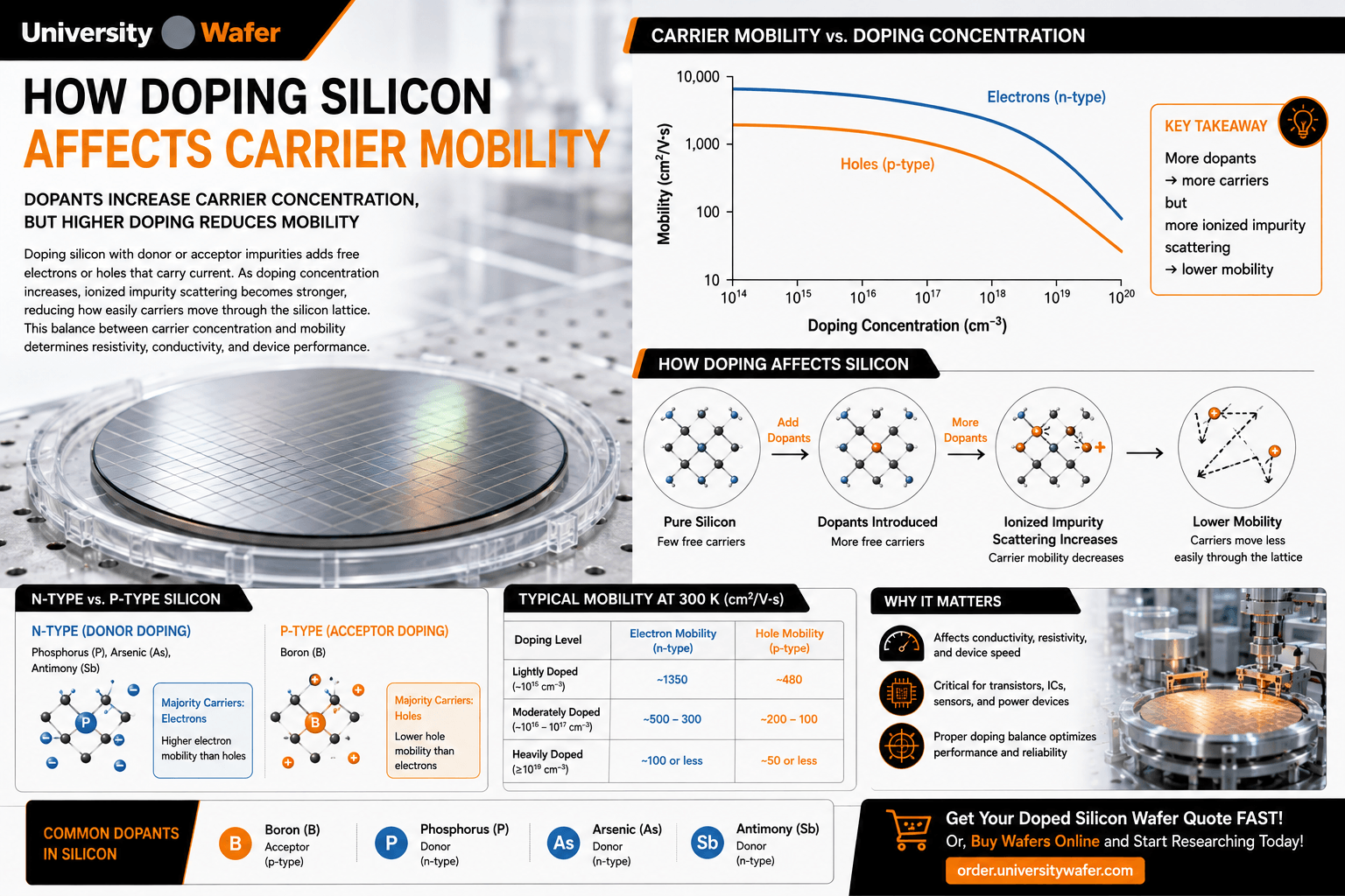
Carrier Mobility at Different Doping Levels
Carrier mobility does not remain constant across all silicon resistivities and doping concentrations. Lightly doped silicon generally provides higher mobility, while heavily doped material typically exhibits lower mobility because ionized-impurity scattering becomes more significant.
| Doping Level | Carrier Mobility | Typical Characteristics |
|---|---|---|
| Lightly Doped | Higher | Less impurity scattering and generally higher resistivity |
| Moderately Doped | Moderate | Balance between carrier concentration and mobility |
| Heavily Doped | Lower | Strong impurity scattering and generally lower resistivity |
Temperature and Carrier Mobility
Temperature also affects carrier mobility. As temperature increases, vibrations within the silicon crystal lattice become stronger. These vibrations, known as phonons, interact with moving carriers and can reduce their mobility.
In lightly doped material and at higher temperatures, lattice scattering can be a dominant mobility-limiting mechanism. In more heavily doped material, ionized-impurity scattering becomes increasingly significant. The relative importance of these mechanisms therefore depends on both temperature and doping concentration.
Why Mobility Matters in Semiconductor Devices
Carrier mobility influences how quickly and efficiently charge can move through a semiconductor. For this reason, mobility is an important parameter when developing transistors, integrated circuits, power devices, sensors, photodetectors, and other semiconductor structures.
For example, the electrical behavior of a field-effect transistor (FET) depends partly on carrier transport within the semiconductor channel. Higher effective carrier mobility can support greater current for a given device geometry and operating condition.
Doping and Silicon Wafer Resistivity
Silicon wafer resistivity is closely connected to dopant concentration. Lightly doped wafers generally have higher resistivity, while increasing the electrically active dopant concentration generally produces lower-resistivity silicon.
However, resistivity cannot be interpreted from carrier concentration alone because mobility also changes with doping. Accurate semiconductor modeling therefore considers both carrier concentration and concentration-dependent mobility.
High-Resistivity Silicon
High-resistivity silicon wafers contain relatively low concentrations of electrically active dopants. These substrates are useful for applications where low free-carrier concentration, reduced electrical loss, or specific dielectric behavior is important.
Applications can include RF research, detectors, sensors, photonics, and specialized semiconductor devices.
Low-Resistivity Silicon
Low-resistivity silicon is more heavily doped to provide increased electrical conductivity. These wafers can be useful when the substrate must provide a conductive path or when particular device structures require highly doped semiconductor regions.
Common Silicon Dopants
Different dopant species can be introduced into silicon to produce either n-type or p-type material. The dopant selected depends on the desired electrical properties and semiconductor fabrication process.
- Boron (B) – Common acceptor used to produce p-type silicon.
- Phosphorus (P) – Common donor used to produce n-type silicon.
- Arsenic (As) – Donor used for n-type silicon and heavily doped device regions.
- Antimony (Sb) – Donor that can also be used to produce n-type silicon.
Carrier Mobility in Semiconductor Research
Understanding the interaction between doping, mobility, resistivity, and carrier concentration helps researchers select substrates with electrical characteristics appropriate for their experiments.
These relationships are important when studying or fabricating:
- MOSFETs and other transistor structures
- Integrated circuits
- Diodes and junction devices
- MEMS and semiconductor sensors
- Photodetectors
- Power semiconductor devices
- Solar cells and photovoltaic devices
- RF and microwave devices
- Semiconductor material characterization
Choosing the Right Silicon Wafer
The ideal substrate depends on more than simply choosing between p-type and n-type material. Researchers should consider dopant species, resistivity, crystal orientation, wafer thickness, surface finish, and device requirements when selecting silicon.
UniversityWafer supplies silicon wafers across a wide range of resistivities, orientations, diameters, thicknesses, dopants, and surface finishes for semiconductor research and device fabrication.