
Did You Know?
The type of silicon wafer you choose can affect device performance. N-type silicon has electrons as majority carriers and is commonly used in high-efficiency solar cell designs. P-type silicon has holes as majority carriers and is widely available for established CMOS and other semiconductor processes.
Factors like resistivity, crystal orientation, and wafer purity can significantly influence minority carrier lifetime, efficiency, and long-term reliability. The right specifications depend on the device architecture and fabrication process.
Get Your Quote FAST! Or, Buy Online and Start Researching Today!
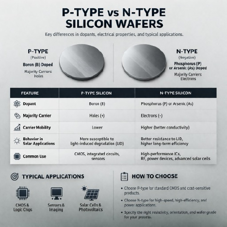
P-Type vs N-Type Silicon Wafers for High Performance Devices
The choice between P-type and N-type silicon wafers plays a critical role in determining the electrical performance, efficiency, and long-term reliability of semiconductor devices. From integrated circuits to high-efficiency solar cells, selecting the correct silicon wafers ensures optimal carrier transport, reduced recombination losses, and consistent fabrication results. Modern semiconductor applications increasingly rely on precise control of dopant type, resistivity, and crystal quality to meet demanding performance requirements.
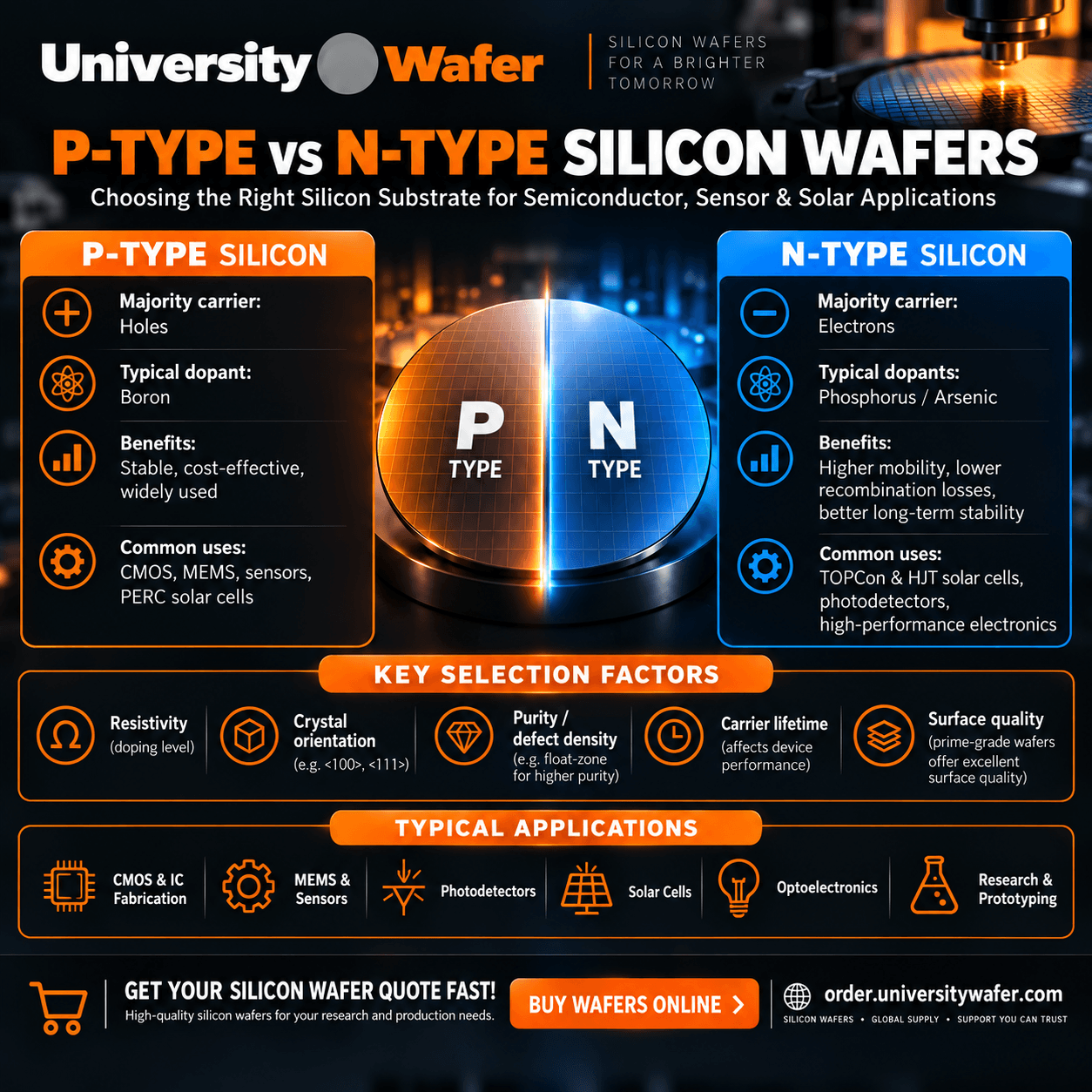
Doping Fundamentals and Electrical Behavior
Silicon conductivity type is controlled by introducing dopants into the crystal or during wafer growth. Boron is an acceptor that makes holes the majority carriers in P-type silicon. Phosphorus and arsenic are donors that make electrons the majority carriers in N-type silicon. Actual device behavior also depends on dopant concentration, junction design, and processing.
P-Type Silicon: Proven and Widely Used
P-type silicon wafers are widely used in established CMOS processes, sensors, MEMS structures, and solar cells. Their availability and cost can make them suitable for large-scale production. Boron-doped, oxygen-containing silicon can experience boron-oxygen-related light-induced degradation (LID) in photovoltaic applications; the extent depends on material quality and cell processing.
N-Type Silicon: Higher Efficiency and Stability
N-type silicon wafers use electrons as majority carriers; electron mobility in silicon generally exceeds hole mobility at comparable conditions. This alone does not determine device switching speed or cell efficiency. N-type wafers avoid the boron-oxygen defect associated with boron-doped silicon and are widely used in advanced solar cell designs, subject to the complete cell structure and processing.
Resistivity and Carrier Lifetime Considerations
Resistivity is a key parameter when selecting a wafer, as it determines how easily current flows through the material. The required resistivity varies by device design: heavily doped, low-resistivity wafers suit some contact and power-device structures, while high-resistivity material can reduce parasitic loss in selected RF or detector applications. Minority carrier lifetime matters particularly in solar cells, where reduced recombination can improve conversion efficiency. Engineers often evaluate these characteristics alongside other silicon wafer properties to ensure optimal device performance.
Crystal Growth Methods and Material Quality
Silicon wafers are commonly produced using Czochralski (CZ) or float zone (FZ) growth methods. CZ wafers are widely used for cost-effective production, while float zone silicon wafers provide higher purity and lower oxygen content. FZ wafers are particularly valuable in research and high-performance applications where minimizing impurities is critical for achieving maximum carrier lifetime and device efficiency.
Surface Quality and Wafer Specifications
Surface finish and thickness uniformity are essential for reliable semiconductor processing. Prime grade silicon wafers offer tight control over total thickness variation (TTV), low surface roughness, and minimal defect density. These characteristics are especially important in advanced lithography and thin-film deposition processes, where even minor surface imperfections can impact yield and performance.
Applications in Solar Cells and Optoelectronics
In silicon solar cell research, N-type wafers are commonly used for high-efficiency TOPCon and heterojunction (HJT) designs, while P-type wafers have been widely used for PERC cells; device architecture and processing determine the final performance. Both materials are also used in optoelectronic devices, including photodetectors and imaging sensors. For photovoltaic research and production, solar wafers are available in multiple grades and doping configurations to support different efficiency and cost targets.
Thin Wafers and Advanced Device Architectures
As semiconductor devices continue to shrink and improve, thinner substrates are becoming more important. thin silicon wafers help reduce material usage while maintaining strong electrical performance. These wafers are particularly useful in flexible electronics, MEMS devices, and next-generation solar cells where reduced thickness can improve efficiency and lower manufacturing costs.
Choosing Between P-Type and N-Type Silicon
The decision between P-type and N-type silicon depends on the application, required doping, resistivity, process flow, and budget. A wafer’s doping type alone does not guarantee higher efficiency or faster device performance. For devices that require a p–n junction, both carrier types are created in the finished structure through growth, diffusion, or implantation. For early-stage development or cost-sensitive projects, test grade silicon wafers can be used for prototyping and experimentation before scaling to higher-grade materials.