Thermal Oxide on Silicon Wafers for Pulsed Laser Deposition
A professor researching Pulsed Laser Deposition (PLD) requested a quote for the following.
I am looking into buying SiO2(200 nm)/Si(100) wafers. I will be using these to grow some films in Pulsed Laser Deposition system. Not familiar with growing on Si (mostly worked on SrTiO3 in the past). I had difficult time choosing which type to choose. Si is not part of the device.
It will be electroded with Al in the lab which will be a bottom electrode for the film. Can you let me know which of the items would be the one that fits the criteria and can you email me a quotation. My colleagues suggested I should be purchasing from your company.
I am flexible in diameter since we will be breaking them into smaller pieces with diamond scribing. The focus is on the film (and Si is not templating it).
It should be intrinsic, oxidized to approximately 200nm SiO2.
100 oriented. One surface should be polished (not sure the level it needs to be - we will sputter 100 nm Al on it before growing the film).
Reference #322474 for specs and quantity.
Get PLD-Ready Substrates Fast
UniversityWafer, Inc. supplies wafers and substrates optimized for Pulsed Laser Deposition (PLD).
Tell us your target material, laser type, and vacuum conditions — we’ll match in-stock or custom wafers that minimize particulates and enhance film uniformity.
Common features:
- Prime and research-grade surfaces
- 1- or 2-side polish with low micro-roughness
- Thermal oxide or nitride coatings
- Pre-cleaned, vacuum-sealed packaging
Accelerate Your Deposition Results
Order pre-cleaned silicon, sapphire, and oxide substrates designed for stable film growth and repeatable results.
Get Your Quote FAST! Or, Buy Online and Start Researching Today!
Recommended PLD Substrates
Custom Surface Preparation
Surface smoothness and cleanliness are critical for achieving uniform film growth in Pulsed Laser Deposition (PLD).
We offer wafers with angstrom-level roughness and optional treatments such as:
- Plasma cleaning and oxide removal
- Buffered oxide etch (BOE) and HF-last surface finishes
- Thermal oxide growth for improved adhesion
- Nitride coatings for diffusion barriers
Wafer Packaging & Handling
All wafers are shipped in vacuum-sealed cleanroom containers to prevent particle contamination and oxidation.
Special packaging options are available for ultra-high-vacuum and reactive materials like MgO and SrTiO₃.
Quick Stock Specs
| Diameter |
Thickness |
Polish |
Options |
| 2"–8" |
~275–625 µm |
SSP / DSP |
Oxide/Nitride, High-Resistivity, Epi-Ready |
| 10–100 mm |
Custom on request |
Research & Prime |
Orientation, Flats, Edge Profiles |
Pulsed Laser Deposition (PLD): How It Works
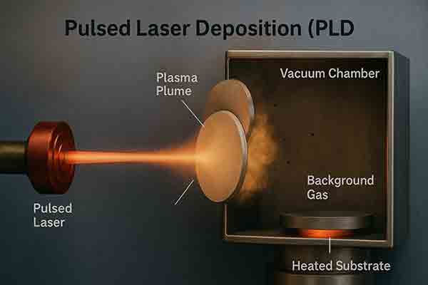
Pulsed Laser Deposition (PLD) is a physical vapor deposition method that uses a high-energy pulsed laser to ablate a solid target. The ablated material forms a plasma plume that expands toward a heated substrate, where it condenses as a thin film. Because the laser pulses deliver energy in short bursts, PLD offers precise control over film composition and growth rate, making it ideal for research in superconductors, ferroelectrics, and oxide electronics.

Laser–Target Interaction
When the focused laser beam hits the target surface, it heats and vaporizes a localized region, ejecting atoms, ions, and clusters into the gas phase. The energy density (fluence) must exceed the material’s ablation threshold, typically in the range of 1–5 J/cm². Shorter laser wavelengths produce smoother ablation and fewer particulates, improving the resulting film quality.
Plume Expansion and Film Formation
The plasma plume contains energetic species that travel through a background gas before reaching the substrate. The composition and density of this plume determine the stoichiometry of the film. Adjusting background pressure and substrate temperature allows researchers to fine-tune the film’s crystallinity, microstructure, and orientation.
Process Parameters that Influence Film Quality
- Laser fluence: Determines ablation rate and particle size.
- Pulse repetition rate: Controls film thickness and uniformity.
- Target–substrate distance: Affects particle energy and film coverage.
- Substrate temperature: Promotes crystallinity and adhesion.
- Ambient gas pressure: Alters plume dynamics and stoichiometry.
Advantages of PLD
PLD can reproduce complex stoichiometries directly from the target, enabling thin films of multicomponent oxides such as YBa₂Cu₃O₇₋ₓ and LaAlO₃. It is valued for its flexibility, clean transfer of material, and compatibility with in-situ monitoring techniques like Reflection High-Energy Electron Diffraction (RHEED). Compared with sputtering or evaporation, PLD enables higher-energy species and superior interface control.
Challenges and Considerations
Despite its benefits, PLD can produce particulates due to splashing from molten target zones. Using off-axis geometries, shorter wavelengths, or substrate rotation minimizes these defects. Scaling the process for large-area uniform films remains a challenge, though modern scanning-beam and multi-target systems address these limitations.
Materials Commonly Grown by PLD
Researchers use PLD to deposit a variety of thin-film materials, including:
- Metal oxides such as ZnO, TiO₂, and SrTiO₃
- Ferroelectric and piezoelectric materials like Pb(Zr,Ti)O₃ (PZT)
- High-temperature superconductors such as YBa₂Cu₃O₇₋ₓ
- Semiconductors and nitrides (Si, GaN, AlN)
- Magnetic oxides and spintronic thin films
Selecting Substrates for PLD
Substrate choice determines film structure, lattice matching, and interface quality. Common PLD substrates include:
Silicon,
Sapphire (Al₂O₃),
Quartz,
MgO, and
SrTiO₃.
Each offers different advantages in lattice constant, transparency, and temperature resistance.
Applications of PLD Films
Thin films created by PLD are used in research and advanced device fabrication, including:
- Superconducting and ferroelectric devices
- Optoelectronic coatings and transparent conductors
- Dielectric and piezoelectric sensors
- Spintronic and quantum materials research
UniversityWafer Support for PLD Research
UniversityWafer, Inc. provides a wide range of substrates compatible with PLD systems, including pre-cleaned, low-defect silicon, oxide-coated wafers, and lattice-matched crystals. We help researchers obtain consistent thin-film results by offering custom wafer specifications and surface finishes tailored to PLD parameters.
Optimizing Deposition Parameters
Each PLD setup behaves differently based on chamber geometry, target composition, and laser wavelength.
Fine-tuning the following factors can significantly improve film uniformity and adhesion:
- Background gas pressure: Adjusting between 10⁻⁶ and 10⁻² Torr helps balance particle energy and stoichiometry.
- Substrate heating rate: Gradual temperature ramping avoids delamination or stress cracking.
- Laser spot size and focus: Determines ablation uniformity and plume density.
- Target rotation: Prevents crater formation and ensures even material removal.
Comparing PLD with Other Deposition Techniques
Unlike sputtering or
CVD,
PLD enables stoichiometric transfer from target to film with minimal compositional deviation.
It also requires smaller material quantities and is ideal for producing multilayered or gradient structures.
Recent Research Trends
Modern PLD systems integrate multi-target carousels and in-situ diagnostics
such as RHEED and optical emission spectroscopy to monitor film growth in real time.
These upgrades have made PLD a cornerstone in materials discovery, especially for quantum oxides and 2D materials.
Example Research Uses
- Developing oxide-based ferroelectric memory devices
- Creating superconducting thin films for cryogenic electronics
- Fabricating transparent conductive oxides for display technology
- Producing piezoelectric films for MEMS actuators and sensors

