ZnO Substrates for Research and Production
Zinc Oxide (ZnO) substrates are widely used in UV/blue optoelectronics, thin-film transistors (TFTs), and sensing devices because ZnO combines a wide bandgap with strong optical transparency and useful electrical behavior when doped. On this page, you’ll find practical examples of how researchers use ZnO wafers and ZnO thin films for LED fabrication, epitaxial growth, STM experiments, and gas sensor development—plus links to compatible glass and deposition methods.
ZnO Wafers to Reseach Light Emitting Diodes
A optics engineer researching LEDs requested the following quote:
I want to see electro-optical and thermo-optical response of ZnO. I would probe it optically by using LEDs in 350-390 nm range and see how external effects (thermal, electrical) change (modulate) probe light (signal from LED).
I would prefer, of course, if you can deposit ZnO on glass with 1 micron thickness. We want to divide film into pixels and investigate optoelectric properities that have good crystal quality. So backing transparent substrate would be fine for us.
I want undoped, (100) orientation and 1 um thickness. And the backing substrate should be transparent between 355-390nm region.
And if you can tell if this could be sliced by wafer cutter, it would be perfect.
UniversityWafer, Inc. Quoted
ZnO(150nm) Coated Soda Lime Glass 1" x1"x 0.7mm
Referece # 224381 for specs and pricing.
Get Your Quote FAST! Or, Buy Online and Start Researching Today!
ZnO Wafers to Fabricate Thin Film Transistor
A chemical engineer requested the following quote:
I am trying to make a thin film transistor with commercial zinc oxide that I can compare with results with our MBE grown zinc oxide.
I was referring to this setups:
-ZnO(50nm) on Fused Silica 10x10x0.5mm
-ZnO(100nm) on Fused Silica 10x10x0.5mm
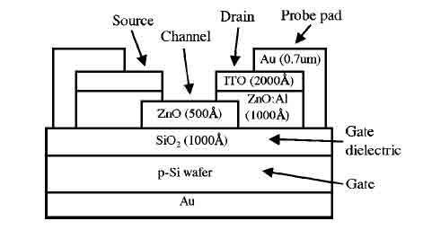
Our TFT model might look like this:

Thin Film Transistor
So I was wondering if the znO on the fused silica meant ZnO on a p-type wafer that has grown some thermal silica on it and then ZnO on top of it (they would be the layers p-Si, SiO2 and ZnO on the figure above). Or it is just fused silica?
Also, do you have any spec sheets on the ZnO for different substrates?
UniversityWafer, Inc. Quoted:
-ZnO(50nm) on Fused Silica 10x10x0.5mm
-ZnO(100nm) on Fused Silica 10x10x0.5mm
Reference #251773 for specs and pricing.
Related ZnO Materials & Thin-Film Deposition Resources
How are Zinc Oxide Substrates Used in LED Fabrication?
Zinc oxide (ZnO) substrates are used in the fabrication of light-emitting diodes (LEDs) primarily because of their favorable electronic and optical properties. ZnO's broad energy gap nails it for LEDs, shining bright from deep blues to UV light. Here's how ZnO substrates contribute to LED fabrication:
-
Wide Bandgap: ZnO has a wide bandgap of about 3.37 eV at room temperature, which allows for  efficient UV light emission. ZnO's knack for efficient UV emission makes it ace for crafting UV LEDs, key in zapping germs in water, sterilizing medical gear, and speeding up the drying process in UV curing.
-
Transparent Conductive Oxide: ZnO is also known for its transparency in the visible spectrum and good electrical conductivity when doped with certain elements (e.g., aluminum or gallium). ZnO shines as a top pick for transparent conductive films in LEDs, letting the light shine through while keeping the electricity flowing.
-
Heterostructure Formation: ZnO substrates can be used to grow various types of semiconductor layers to form heterostructures, which are critical for the operation of LEDs. By trapping electrons and holes right where they need to be, these layers really crank up the brightness of the light we see.
-
Epitaxial Growth: The epitaxial growth of semiconductor layers on ZnO substrates is a key process in LED fabrication. Materials like GaN (Gallium Nitride) and its alloys, which are commonly used in blue and UV LEDs, can be grown on ZnO substrates. ZnO substrates are a solid pick because they sync well with GaN materials, leading to top-notch layers for LEDs that shine bright and last long thanks to fewer flaws.
-
Optical Properties: ZnO has strong luminescence, which can be leveraged in LEDs. ZnO's knack for emitting bright light when its electrons and holes recombine boosts the performance of LEDs, lighting them up brilliantly.
-
Flexibility and Cost: ZnO substrates can be produced through several low-cost methods, including sputtering and chemical vapor deposition, making them economically attractive for LED fabrication. Tweaking the electrical properties of ZnO substrates is key, as it lets you dial in specific performance features for LEDs without breaking the bank.
So, when it comes down to why we pick ZnO for making LEDs, it's really about their stellar ability to handle UV light, top-notch electrical and glowing traits, plus they're spot-on for layering with other semiconductors. So, these traits let us crank out top-notch LEDs that really shine when you need UV or blue light—for all those techy uses.
ZnO Cyrstals for STM Experiments
A PhD candidate requested a quote for the following:
We are interested in ZnO(0001) 10x10x1 mm crystals with and without Ga doping. Want to use for STM experiments so surface has be to very good. Your web site suggests that you can provide both Zn and O-terminated crystals – would like to more about those surfaces.
Reference # 254411 for specs and pricing.
ZnO Grown on Gallium Nitride Single Crystal Wafers
A PhD student requested the following:
Can you give me information about the crystallinity of GaN single crystals in terms of Omega scans / rocking curves of the 0002 reflex? I would like to use the GaN single crystal for the epitaxial growth of ZnO.
Reference #257413 for specs and pricing.
What ZnO Substrates are Used to Fabricate Gas Sensor?
A graduate student requested the following:
I need a glass substrate for my research project. I am going to deposit gold on this substrate and use it as an electrode for a gas sensor. The sensing material would be ZnO. I would be appreciated if you can help me find the best substrate. I don't know the differences between different kinds of glass substrates that you have on your website.
For your research project where you plan to deposit gold on a substrate to use as an electrode for a gas sensor with ZnO as the sensing material, selecting the appropriate glass substrate is crucial for optimal performance and reliability of your sensor. Here are some considerations and recommendations:
-
Fused Silica or Quartz Glass: These materials are highly recommended for applications requiring thermal stability and low thermal expansion. Fused silica has excellent transmission in the UV range, which might be beneficial depending on your detection methods or if UV treatment is part of your process. It also has good chemical resistance, making it suitable for various deposition and etching processes.
-
Borosilicate Glass: This type of glass is known for its low coefficient of thermal expansion, making it resistant to thermal shock. It's a good choice if your fabrication process involves significant temperature changes. Borosilicate glass, like the commonly known brand Pyrex, offers good chemical stability and is less expensive than fused silica.
-
Soda-Lime Glass: This is the most common type of glass and is less expensive compared to fused silica and borosilicate glass. However, it has a higher coefficient of thermal expansion and may not be as suitable for high-temperature processes. It can still be used if your processing conditions are mild and cost is a significant factor.
-
Aluminosilicate Glass: This type of glass, which includes brands like Gorilla Glass, is known for its durability and scratch resistance. It has a thermal and chemical stability that falls between borosilicate and soda-lime glasses. It could be a good choice if mechanical durability of the substrate is a concern.
-
Considerations for Gold Deposition: Ensure that the glass substrate you choose can withstand the deposition process of gold, whether it's Physical Vapor Deposition (PVD), Chemical VaporDeposition (CVD), or sputtering. The substrate should also be compatible with any adhesion layers you might need to apply before gold deposition.
-
Surface Quality and Preparation: The surface quality of the glass substrate can significantly affect the performance of your gas sensor. A smooth, clean surface is essential for uniform gold film deposition. Consider substrates that can be easily cleaned and, if necessary, polished to reduce surface roughness.
Given the requirements for thermal stability, chemical resistance, and suitability for gold deposition, fused silica or quartz glass seems to be the best choice for your application. It offers excellent properties for high-precision and high-temperature applications and is compatible with ZnO as a sensing material. However, consider your project's specific requirements, including the deposition method, operating temperature range, and budget, when making your final decision.
Reference #260701 for specs and pricing.


 efficient UV light emission. ZnO's knack for efficient UV emission makes it ace for crafting UV LEDs, key in zapping germs in water, sterilizing medical gear, and speeding up the drying process in UV curing.