Request Research Substrates
Interested in testing semiconductor or optical thin-film materials in your next research project? Fill out the form below to receive a fast, personalized quote from UniversityWafer.com. We supply wafers and substrates for aerospace, vacuum, and microgravity-related R&D missions.
Ready to explore space-informed thin films? Tap our inventory, request special substrate sets, or ask for documentation templates that support proposal writing and flight-like testing.
Get Your Quote FAST! Or, Buy Online and Start Researching Today!
Educational Insight
In space, the absence of convection means thin films grow in a unique environment where atoms and molecules arrange more evenly across the substrate. Researchers can measure stress, uniformity, and electrical behavior of materials in ways impossible on Earth.
These experiments help scientists design radiation-resistant semiconductors, optical coatings for satellites, and quantum-grade materials for space-based computing and sensing. The ISS has become not just a platform for astronauts— but a laboratory for material scientists worldwide.
As missions expand, UniversityWafer.com aims to make high-purity Si, GaAs, InP, ZnSe, LiNbO3, and other advanced substrates available for zero-gravity thin-film growth and surface analysis.
Thin-Film Research in Space
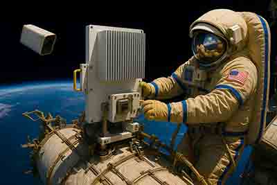
Microgravity offers a rare laboratory for materials science: without buoyancy-driven convection and sedimentation, thin films can nucleate and grow in ways that are difficult to reproduce on Earth. On the International Space Station (ISS), researchers can observe film morphology, defect formation, and interfacial chemistry with fewer gravity-related perturbations. That means more controlled layer-by-layer growth, improved uniformity across the wafer, and new insights into stress, grain boundaries, and crystallographic texture that ultimately influence device yield and performance. These orbital campaigns are not just demonstrations; they are building a foundation for higher-purity films for sensors, photonics, radiation-hardened electronics, and quantum devices.
![]()
Where UniversityWafer.com Can Help
UniversityWafer.com already supports advanced R&D with research-grade wafers and substrates—silicon (CZ, FZ, and SOI), Sapphire, GaAs, InP, LiNbO3, LiTaO3, ZnSe, and more—specified by orientation, dopant, resistivity, thickness, TTV, bow/warp, and surface finish (double-side polished, epi-ready). As space-based studies expand, we envision supplying curated substrate sets prepared for flight-like environments: ultra-clean packaging, traceable documentation, and process notes tuned for physical vapor deposition (PVD), chemical vapor deposition (CVD), atomic layer deposition (ALD), and molecular beam epitaxy (MBE). By aligning wafer spec, metrology, and handling with the constraints of orbital hardware, we aim to reduce pre-flight variability and accelerate experiment readiness.
Why Microgravity Matters for Films
In orbit, the absence of gravity-driven flows alters mass transport and thermal gradients during deposition and post-deposition anneals. Researchers can decouple convective effects from diffusion and surface kinetics, revealing rate-limiting steps that are obscured on Earth. The resulting data can inform models for nucleation density, island coalescence, and step-flow growth, helping teams design recipes that translate back to terrestrial tools with improved uniformity and fewer embedded defects. Equally important, microgravity can clarify how multilayer stacks accumulate stress and how interfaces evolve—key to adhesion, electromigration resistance, optical loss, and superconducting coherence.

Candidate Substrates & Use Cases
For electronics and MEMS, Si and SOI provide a stable platform to study seed layers, diffusion barriers, and metallization relevant to lift-off and damascene processes. For high-frequency and optoelectronic work, metallized contact stacks on dielectric oxides or wide-bandgap materials can probe adhesion and stress in low-defect regimes. LiNbO3 and LiTaO3 support low-loss photonics and acousto-optic films, while GaAs, InP, and ZnSe enable infrared/visible optoelectronics and sensor coatings. Each material family benefits from controlled microstructure and interface engineering that microgravity can uniquely illuminate.
Packaging, Cleanliness & Documentation
Flight-adjacent materials work demands rigorous cleanliness, labeling, and traceability. Our vision includes wafer carriers sealed for low-particle transport, pre-clean protocols (e.g., solvent and DI sequences with verified NVR), and optional ozone or UV treatments prior to loading into vacuum hardware. We can provide lot-level certificates noting orientation, flats/notches, micro-roughness, oxide/nitride presence, and pre/post metrology (thickness, resistivity, haze, AFM/RMS where applicable). The goal is simple: remove ambiguity so the only variable under test is the physics of thin-film formation in microgravity.
From Orbit Back to Earth
Results from orbital trials should transfer to ground tools—often with tighter process windows and improved repeatability. By pairing space-derived insights with terrestrial deposition (e.g., tuning pressure, plasma density, or precursor flow to emulate reduced convective effects), labs can reach lower defectivity and better film stoichiometry at scale. UniversityWafer.com’s role here is to keep substrate supply and documentation consistent across both environments so your data sets remain comparable and statistically meaningful.
Collaboration & Next Steps
Planning a proposal or scoping a pilot? We can assemble wafer kits tailored to your hypothesis (orientation/miscut for step-flow studies, oxide/nitride masks for lift-off comparisons, or multi-material sets for interface experiments). We’ll help map substrate specs to your deposition and characterization plan—profilometry and AFM for roughness, XRD for texture and strain, ellipsometry for thickness/optical constants, and four-point probe for sheet resistance—so your pre- and post-flight data align. When you’re ready to move forward, we’ll prepare quotes, timelines, and documentation that fit academic, government, or commercial compliance requirements.
Ready to explore space-informed thin films? Tap our inventory, request special substrate sets, or ask for documentation templates that support proposal writing and flight-like testing.
