
Understanding Silicon Wafer Surface Roughness
Silicon wafer surface roughness refers to microscopic variations in surface height that remain after wafer slicing, lapping, etching, and polishing. Although a polished silicon wafer may appear perfectly smooth to the human eye, nanoscale peaks and valleys can still be detected using precision surface characterization techniques.
Surface roughness is especially important in semiconductor research because the quality of the silicon surface can influence thin-film uniformity, wafer bonding, lithography, electrical interfaces, optical behavior, and device performance. Researchers therefore select wafers with surface finishes appropriate for their specific fabrication or characterization process.
How Is Silicon Wafer Roughness Measured?
Two commonly reported parameters for wafer surface characterization are Ra and RMS (Rq) roughness. These values describe surface-height variations relative to an average or reference surface.
- Ra (Average Roughness): The arithmetic average of the absolute surface-height deviations measured across a specified area or profile.
- Rq or RMS Roughness: The root mean square of the surface-height deviations. RMS measurements give greater weight to larger peaks and valleys.
Because roughness values depend on measurement area, instrument resolution, filtering, and scan conditions, researchers should consider the measurement method when comparing specifications between silicon wafers.
Atomic Force Microscopy (AFM) for Silicon Wafers
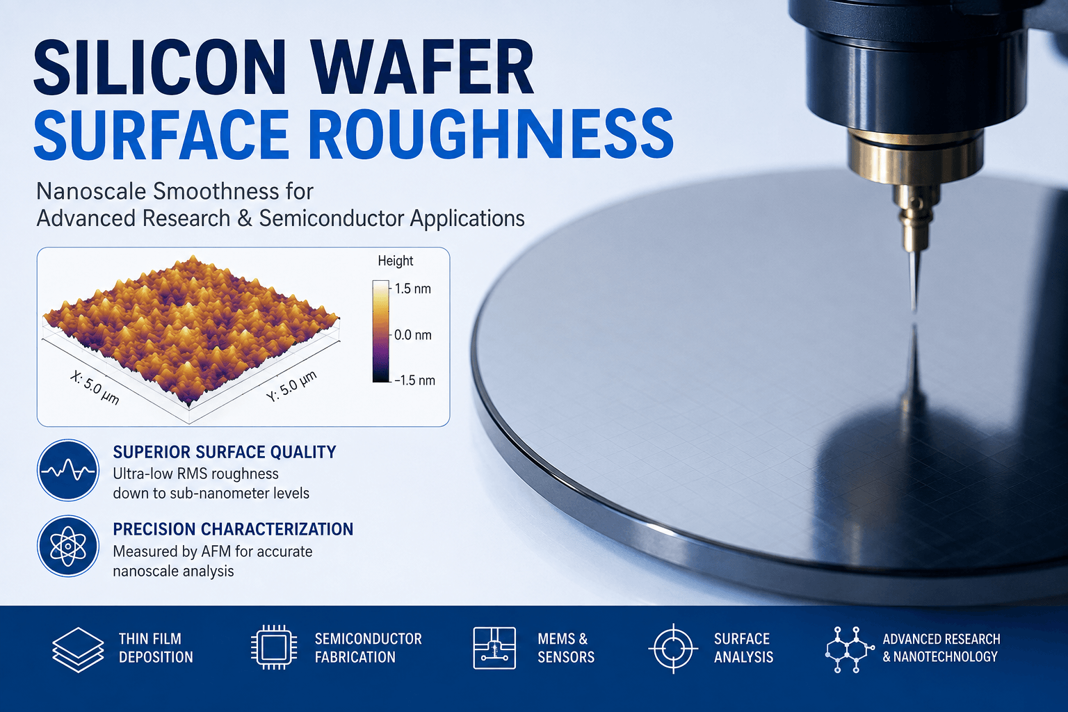
Atomic Force Microscopy (AFM) is widely used to characterize nanoscale silicon wafer surfaces. An AFM scans a very small probe across the wafer and records variations in surface height, producing a three-dimensional representation of the surface topography.
AFM measurements can reveal nanoscale features that conventional optical inspection cannot resolve, including polishing marks, particles, pits, scratches, local defects, and changes caused by surface processing. Researchers can use the resulting data to calculate parameters such as Ra and RMS roughness.
Why Low Surface Roughness Matters
An ultra-smooth silicon wafer surface provides a more controlled starting substrate for many semiconductor and materials-science processes. Excessive roughness can affect how materials are deposited, patterned, bonded, or characterized at the wafer surface.
Low-roughness silicon wafers are particularly useful for applications such as:
- Atomic Force Microscopy (AFM) studies
- Thin-film deposition and characterization
- Photolithography and microfabrication
- MEMS and microsensor fabrication
- Wafer bonding experiments
- Surface chemistry and functionalization
- Graphene and other 2D-material research
- Optical and photonic research
- Nanotechnology and nanoscale device fabrication
How Polishing Reduces Silicon Surface Roughness
Silicon wafers undergo several processing steps before reaching a polished surface suitable for advanced research. After a silicon ingot is sliced into individual wafers, mechanical and chemical processes are used to remove saw damage and improve wafer flatness and surface quality.
Chemical Mechanical Polishing (CMP) combines chemical reactions with controlled mechanical polishing to produce a highly planar and smooth silicon surface. Proper polishing can significantly reduce surface irregularities while preparing the wafer for subsequent semiconductor processing.
Single-Side and Double-Side Polished Silicon Wafers
Single-side polished (SSP) silicon wafers have one highly polished device surface, while the opposite side typically has a different surface finish. SSP wafers are widely used when fabrication or characterization is performed primarily on one side of the substrate.
Double-side polished (DSP) silicon wafers have polished surfaces on both sides. DSP substrates are useful for applications requiring optical transmission, backside processing, wafer bonding, precision metrology, MEMS fabrication, or highly controlled surfaces on both sides of the wafer.
Choosing Silicon Wafers for Surface-Sensitive Research
Surface roughness is only one specification to consider when selecting a silicon substrate. Researchers may also need to specify wafer diameter, crystal orientation, thickness, resistivity, conductivity type, dopant, total thickness variation (TTV), bow, warp, oxide thickness, and whether the substrate requires single-side or double-side polishing.
Selecting the appropriate combination of silicon wafer surface quality and material specifications provides a consistent substrate for experiments where nanoscale surface characteristics can influence results.
Get Your Low-Roughness Silicon Wafer Quote FAST! Or, buy online and start researching today!
What Is a Typical Silicon Wafer Surface Roughness?
The surface roughness of a silicon wafer depends on the wafer grade, polishing process, surface treatment, and measurement method. Prime-grade silicon wafers are manufactured with highly polished surfaces suitable for demanding semiconductor and research applications where nanoscale surface quality is important.
For many polished silicon substrates, surface roughness is evaluated at the nanometer or sub-nanometer scale. Researchers requiring especially smooth surfaces should specify the required Ra or RMS roughness together with the scan size and measurement technique rather than relying only on a general "polished" specification.
Surface Roughness and Silicon Wafer Grade
The required surface finish often depends on the intended application. Prime-grade silicon wafers are typically selected for processes requiring excellent surface quality, dimensional control, and low defect levels. Test and mechanical-grade wafers may be appropriate when extremely low surface roughness is not essential.
Researchers performing deposition, lithography, bonding, or nanoscale characterization should carefully evaluate wafer grade and polishing requirements before selecting a substrate.
Surface Roughness vs. Wafer Flatness
Surface roughness and wafer flatness are different specifications. Roughness describes microscopic surface-height variations over a relatively small measurement area, while flatness parameters characterize larger-scale dimensional variations across the wafer.
Specifications such as Total Thickness Variation (TTV), bow, and warp describe wafer geometry rather than nanoscale texture. A wafer can therefore have an extremely smooth polished surface while still exhibiting measurable large-scale thickness or shape variation.
Surface Roughness and Thin-Film Deposition
Surface condition can influence the behavior of deposited materials. A smooth and properly prepared silicon substrate provides a controlled starting surface for thin-film deposition, including dielectric, semiconductor, metallic, and research coatings.
For very thin films, nanoscale substrate features may influence film morphology, interface quality, nucleation, and characterization results. Researchers working with thin films should therefore consider both the initial wafer roughness and any surface changes introduced during cleaning or processing.
Surface Roughness After Thermal Oxidation
Silicon wafers are frequently used with thermally grown silicon dioxide. Thermal oxide on silicon wafers provides an electrically insulating and chemically stable SiO2 layer for semiconductor fabrication, MEMS, sensors, and materials research.
The final surface characteristics can depend on the original silicon surface as well as oxidation and subsequent processing conditions. When nanoscale roughness is critical, researchers may characterize the substrate before and after oxidation to determine how processing affects surface morphology.
Wafer Cleaning Before Surface Measurements
Surface contamination can interfere with accurate roughness measurements. Organic residue, particles, photoresist, native oxide, and other contaminants may appear as surface features during AFM or profilometry.
Appropriate silicon wafer cleaning can help prepare substrates for surface characterization and subsequent fabrication. The cleaning procedure should be selected carefully because aggressive chemical or physical treatments can alter the surface being investigated.
AFM vs. Profilometer Measurements
Atomic Force Microscopy (AFM) on silicon wafers is particularly useful for studying nanoscale topography and calculating roughness parameters over small scan areas. AFM can reveal extremely small surface features that may not be visible using conventional microscopy.
A profilometer can also provide valuable surface information, particularly for measuring larger features, steps, film thickness differences, and surface profiles. The most appropriate measurement technique depends on the lateral dimensions and vertical scale of the features being investigated.
Surface Roughness for Wafer Bonding
Surface quality becomes especially important when two wafers must form an intimate interface. Excessive roughness, particles, or contamination can reduce the effective contact area between surfaces and interfere with successful bonding.
Low surface roughness, good wafer flatness, and appropriate cleaning are therefore important considerations for direct bonding and other advanced substrate-integration techniques. Silicon-on-insulator (SOI) wafers are an important example of engineered silicon substrates used for MEMS, photonics, electronics, and advanced device research.
Surface Roughness for MEMS and Nanotechnology
Surface characteristics can become increasingly significant as device dimensions decrease. In MEMS research, nanotechnology, biosensors, and microfabrication, substrate quality can influence interfaces, deposited layers, mechanical structures, and measurement repeatability.
For surface-sensitive experiments, researchers should define the required roughness specification and measurement conditions when ordering wafers. UniversityWafer can supply silicon substrates with a range of diameters, orientations, resistivities, thicknesses, dopants, oxide layers, and polishing configurations for research and development.