What Wafers Used to Perform Electron Beam Lithography?
A international company requested a qutoe for the following wafers:
Silicon Nitride (SiN) I would like to get 10 units,
100 mm wafers consisting of a layer of Si3N4 (LPCVD deposition) of thickness 550 nm placed on top of a SiO2 layer of 2 um (or 3um) on top of a Si substrate.Double side polished.
For the Silicon Carbide, we are interested in 10 units.
10 mm x 10 mm wafers consisting of a layer of Silicon Carbide of thickness 500 nm placed on top of a SiO2 layer of 2 um (or 3um) on top of a Si substrate.Double side polished.
We want to perform electron beam lithography on those samples.
I would like to know if you could make the deposition of amorphous silicon carbide, I think the samples that are displayed on the website are SiC like a crystal.
Please reference #270702 for pricing.
Get Your Quote FAST! Or, Buy Online and Start Researching Today!
Fused Silica for Electron Beam Lithography
A PhD candidate from an east coast university requested a quote for the following:
We are looking for fused silica wafers, either JGS1 or JGS2, 1 inch diameter, 500 um thickness, double side polished. I did not see that part on your website but I was told we bought from you in the past. If you can supply such, could you please send me an offer for 50 and 100 pieces?
1 inch diameter, we will use them as substrates for electron beam lithography.
Reference #266349 for pricing.
Key Terms Used in Electron Beam Lithography
- nanopatterned uv
- nanoparticle deposition
- nanostructure deposition
- metal nanostructures
- metal nanocrystals
- beam lithography
- localized nanoparticle
- fabrication capabilities
- characterization techniques
- electron microscopy
- lithography method
- process fabrication
- lithography technique
- fabrication technique
- resistant metal
What Is Electron Beam Lithography
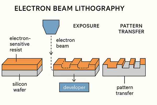
Electron Beam Lithography (EBL) is a high-resolution patterning technique used in micro- and nanofabrication. It uses a tightly focused beam of electrons (instead of light, as in photolithography) to directly write custom patterns onto a resist-coated substrate, such as a silicon wafer.
Key Characteristics:
-
Resolution: Can achieve feature sizes down to a few nanometers.
-
Flexibility: Ideal for research and prototyping since it does not require masks.
-
Speed: Slower than optical lithography due to its serial writing process.
How It Works:
-
Substrate Preparation: A wafer (e.g., silicon) is coated with an electron-sensitive resist, like PMMA (polymethyl methacrylate).
-
Exposure: The electron beam scans across the surface and modifies the solubility of the resist in the exposed regions.
-
Development: The exposed (or unexposed, depending on resist type) areas are removed in a developer solution.
-
Pattern Transfer: The developed pattern can be etched or used for material deposition.
Substrates Used For The Following Applications
Here are the typical silicon wafer specifications used for each of the applications you listed:
1. Nanostructure Fabrication
2. Quantum Dot Arrays
-
Diameter: 100 mm or smaller (e.g., 50.8 mm for test runs)
-
Type: Undoped or intrinsic silicon
-
Orientation: ⟨100⟩ for uniform electronic properties
-
Resistivity: Very high (>10,000 Ω·cm)
-
Surface: Atomically smooth DSP surface; epi-ready optional
-
Note: SOI (Silicon-on-Insulator) wafers are often used for vertical confinement
3. Photonic Crystals
-
Diameter: 100 mm or 150 mm
-
Type: SOI wafers preferred (device layer: 200–300 nm typical)
-
Orientation: ⟨100⟩
-
Doping: Lightly doped or intrinsic
-
Surface: DSP, with top layer optimized for etching photonic structures
-
BOX Thickness: 1–3 μm buried oxide layer depending on design
4. Semiconductor Device Prototyping
-
Diameter: 100 mm, 150 mm, or 200 mm
-
Type: Prime-grade, CZ
-
Orientation: ⟨100⟩ standard
-
Doping: n-type or p-type (Boron or Phosphorus), depends on device
-
Resistivity: 1–10 Ω·cm typical for CMOS/MOSFETs
-
Surface: Single-side polished (SSP) or DSP for multilayer builds
5. MEMS and NEMS Development
-
Diameter: 100 mm or 150 mm (lab use), 200 mm (industrial)
-
Type: SOI wafers or thick DSP CZ wafers
-
Orientation: ⟨100⟩ or ⟨110⟩ for anisotropic etching
-
Doping: Lightly doped or intrinsic for mechanical stability
-
Device Layer (SOI): 1–100 μm depending on structure thickness
-
BOX Layer: 1–3 μm for MEMS release processes
-
Handle Wafer: Thick for structural support (500+ μm)
Advantages:
Limitations:


