Need to try a wafer spec but don't want to spend for 25 wafers? Now you can!
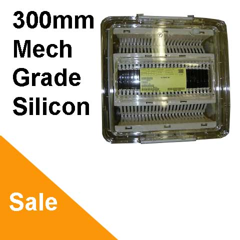
We have a large selection of Prime, Test and Mechanical GradeSilicon wafers
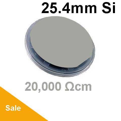
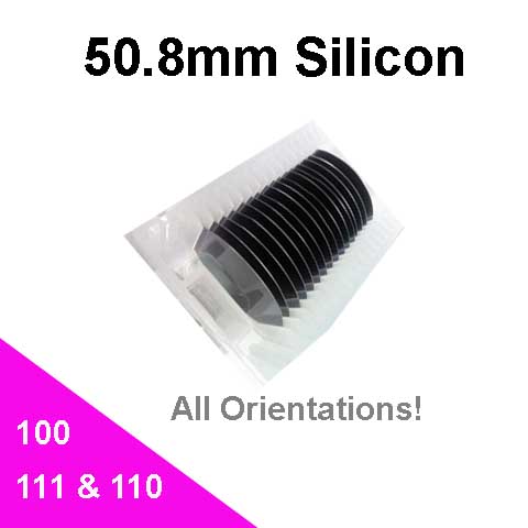
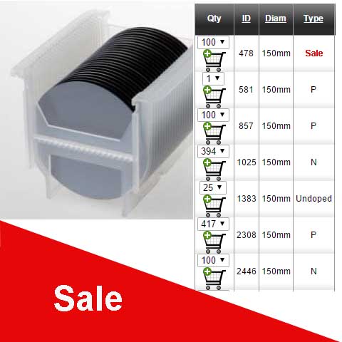
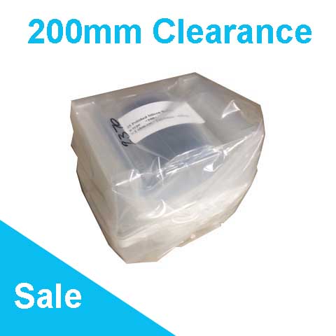
1" - 12" Silicon Wafers low doped and highly doped in stock and ready to ship. Examples full and partial silicon wafer cassettes include:
Just Some of our Silicon Wafer Inventory
"The (silicon) wafers have arrived today, and we really pleased with them! Thumbs up to your production crew!"
Researcher from University of Exeter Free Silicon Wafer Support on All Substrates!
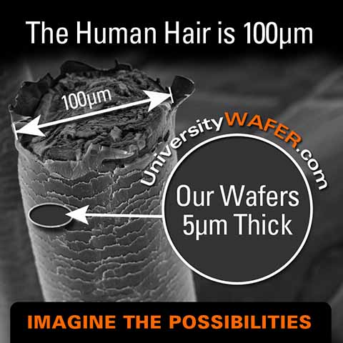
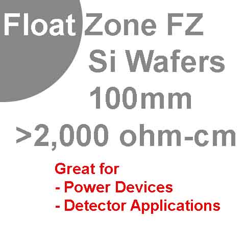
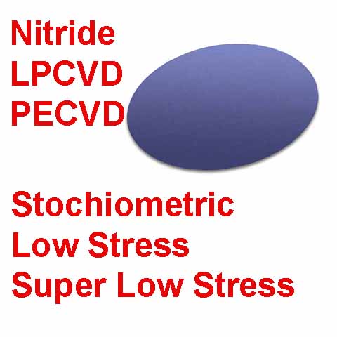
A. We have Ultra-Flat Silicon with the following spec Prime Silicon Wafers 100mm P-type /Boron doped <1-0-0> 490-510 micron 0.005-.020 ohm-cm Semi Std Double Side Polished Total Thickness Variation (TTV)<1 um. These are great for making SOI or MEMS!
Q. What is the roughness value (rms) silicon wafer?A. The majority of our Prime Grade wafers have a roughness value Ra<5Å .
Q. What is the definition of silicon wafers?A. A Si wafer, or substrate, or silicon is grown in a tube from a seed into a long ingot that is then sliced into various thicknesses used in electronics for the fabrication of integrated circuits and in photovoltaics. The wafer serves as the substrate for microelectronic devices built in and over the wafer and undergoes many microfabrication process steps such as doping or ion implantation, etching, deposition of various materials, and photolithographic patterning. Finally the individual microcircuits are separated (dicing) and packaged.
Q. Do you sell platinised silicon wafers?A. Yes! We sell Platinised and thin films of almost all the metals! Just let us know the specs and quantity for an immediate quote!
Q. Do you sell one silicon wafer? If so, how?A. Yes! We sell as few as one Silicon wafer. We sell in individual wafer carrier.
Q. How do you clean Si 100 wafer before silicon dioxide is formed for bump production?A. The RCA clean is a standard set of wafer cleaning steps which need to be performed before high-temperature processing steps (oxidation, diffusion, CVD) of silicon wafers in semiconductor manufacturing.
Werner Kern developed the basic procedure in 1965 while working for RCA, the Radio Corporation of America.[1][2][3] It involves the following chemical processes performed in sequence:
Removal of the organic contaminants (organic clean + particle clean)
Removal of thin oxide layer (oxide strip, optional)
Removal of ionic contamination (ionic clean)
A. Yes! We can laser down the wafer so you could get two 100mm from one 200mm wafers including flats!
Q. What is silicon wafer reclaim?A. It's when you have a wafer that has thin films or oxide etc on them and we strip and clean them so the wafers can be reused.
Which keyword did you use to find us? Tell us and you'll receive a discount on your order!
Silicon wafer vendor