Wet Thermal Oxide as Holders in RIE Processes
A nanofabrication researcher requested the following quote:
We are interested in purchasing some 4 inches SiOx wafers to be used as holders in RIE processes. We are interested in having thick layers of thermal oxide, and we have seen that you offer up to 1 um in thickness (is it your definitive upper limit?).
We would be very grateful if you could send us an offer for a box of 25 wafers with ID=2006, as well as an estimation for the delivery charge.
Reference #210330 for specs and pricing.
Why Grow Thermal Oxide Onto Silicon Wafer's Surface?
The combination of silicon wafers and thermal oxide allows for many more things than just heat transfer. These include better conductivity, higher bandwidth, and even better insulation. However, the biggest thing that thermal oxide can offer is a structural change in objects, making the material stronger and more durable. The oxide is able to change the electronic charges on any surface, changing its charge structure in the process. This results in greater strength and less susceptibility to indentation and bending. This makes the material better suited to use in things like mechanical seals, where the properties are best served by a change to a new material.
Get Your Silicon Quote FAST! Or, Buy Online and Start Researching Today!
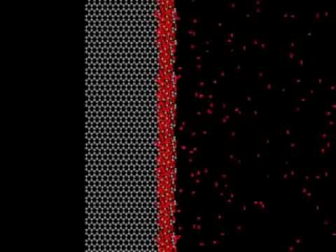
Wet and Dry Oxide Explained
Many companies use thermal oxides for a wide range of purposes, including dry cell batteries. These have the potential to be high performance, extremely safe, and environmentally sound. But which type is best suited for your needs? There are many types, all of which are well suited for specific applications, so here is a brief overview of the main types of thermal oxides on the market today.
 Wet Vapor-Grown: This is probably the most common of the types of thermal oxide, and is generally the one used for the majority of products. Wet thermal oxide usually uses wafer liquid that is grown on the wafer's crystalline structure. As the liquid evaporates, the crystals fall with it, creating a layer of solid oxide. When this layer dries, the oxide continues to grow, becoming a perfectly dry film. Wet thermal oxide, however, can be grown without using wafers, allowing it to be used in other areas.
Oxidizing Metals: A substrate is typically made of one of four different elements: silicon, boron, phosphorous or oxygen. Silicon is the most popular for oxidizing because it is the most commonly found element in thermal oxide. Other elements can be added as substrate materials, but in most cases silicon and boron are the most commonly used. Oxidizing the metal substrate increases the surface area of the cells in a cell, while at the same time reducing the rate of corrosion.
Phosphorus is the most commonly grown phosphorescent mineral in thermal oxidation. Its high solubility and great conductivity make it a great choice. The phosphorous also allows the oxygen in thermal oxidation to pass through the structure more easily, which allows it to have a much fresher and cleaner burn. As the temperature and time progresses, the phosphorous layer will slowly grow a thin layer of oxide on the bare silicon surface, becoming a crystal structure.
Phosphorus also has another great benefit. Because it allows the silicon wafer to be porous in areas where it doesn't normally get water, it acts as a scale inhibitor. This means that it doesn't allow the area to get too hot or too cold, making it more stable for the micro-structure development that is taking place. With less heat forming a complete wet oxide layer, the micro-structure is able to grow thicker and last longer than if the structure was not damp.
Oxygen Phosphide: Another type of material that can be used as a substrate for wet thermal oxide wafers is silicon dioxide. Silicon dioxide is similar to phosphorus in many ways, except that it doesn't form a oxide coating. It does, however, have its advantages. It is extremely smooth, which allows for smooth movement within the micro-structure.
It also has a very high density, which allows for a greater amount of moisture to move into the wafer surface. Because of this, the moisture content is much less than with dry oxides. For this reason, the wafer surface is able to stay flat for a longer period of time, thus improving stability. Also, because the dry oxide is still a liquid, it never becomes too hot or too cold, which allows for better transfer of thermal energy across the surface.
120 Angstroms of Dry Oxide
A PhD candidate requested a quote for the following.
We are interested in growing a 120 Å thick SiO2 layer on silicon wafers using dry oxide. Could you please provide information on whether you can assist with this? If so, what would be the price per unit for 4-inch and 6-inch wafers? Additionally, what is the lead time for this service? Please let us know at your earliest convenience so we can plan accordingly.
We need to grow 120 Angestrom of SiO2 on the Silicon wafer, with high uniformity. If you can let us the price and the non-uniformity percentage, that would help us to make a decision. The quantities of wafers are expected to be around 15 wafers.
UniversityWafer, Inc. Quoted:
- 4'' dia. 120 Å thick SiO2 layer on silicon wafers using dry oxide,high uniformity <50%
- 6'' dia. 120 Å thick SiO2 layer on silicon wafers using dry oxide,high uniformity <50%
Reference #320264 for specs and pricing.
Wet Thermal Oxide Used as Holder for Deep Reactive Ion Etch
A university laboratory manager requested a quote for the following:
Could you give me an inventory of the wafers you have at the moment? I am thinking about getting one casette of 3" silicon wafer and 4" silicon wafer to make microposts to study wetting behaviour, i.e.
electrical properties are not important. I am also interested in getting 5" wafer with thick thermal oxide, to use as a holder for Deep reactive ion
etch. Can you recommend how thick the thermal oxide should be for this purpose? and what is the min. number of 5" wafer can I buy?
Reference #211734 for specs and pricing.
What are the Differences Between Wet and Dry Thermal Oxide?
A distinguished professor of a physics and astronomy department asks what is the difference between dry oxide and thermal oxide? I just want make sure SiOx layer could be used as the gate dielectric for our field effect transistors.
Both "dry oxide" and "thermal oxide" refer to silicon dioxide (SiO2) layers that are grown on silicon wafers, primarily used in semiconductor device fabrication. The difference between the two lies in the method of growth and the properties of the oxide:
-
Method of Growth:
-
Dry Oxidation: In this method, silicon wafers are exposed to dry oxygen (O2) at high temperatures to form silicon dioxide. The reaction can be simplified as: Si+2H20→SiO2+2H2
-
Thermal Oxidation: The term "thermal oxidation" is a broader category that includes both dry and wet oxidation processes. In wet oxidation, silicon wafers are exposed to water vapor (H₂O) at high temperatures. The reaction can be simplified as:Si+2H2O→SiO2+2H2
Wet oxidation typically grows oxide faster than dry oxidation and results in a slightly different oxide quality.
-
Properties:
- Dry Oxide:
- Grows more slowly than wet oxide.
- Produces a denser, higher-quality oxide layer with fewer imperfections and lower defect density.
- It's often used in applications where a thin, high-quality oxide layer is needed, such as gate oxides in MOSFETs.
- Wet Oxide (a type of thermal oxide):
- Grows faster than dry oxide.
- Has slightly higher defect densities and is less dense than dry oxide.
- Often used for thicker oxides or in applications where growth speed is more critical, such as field oxides or isolation regions.
-
Applications:
- Dry Oxide: Commonly used for gate oxides in MOSFETs due to its superior quality.
- Wet Oxide: More suited for areas where thicker oxide layers are needed quickly, like field oxides.
To summarize, while both dry and thermal oxides are grown through high-temperature processes on silicon, the distinction primarily lies in the oxidizing agent (O₂ vs. H₂O) and the resulting properties of the oxide. It's worth noting that "thermal oxide" as a term can technically encompass both dry and wet oxides, but when comparing the two, it's often referring to the wet oxidation process.
The Purpose Of Growing Thermal Oxide Onto Silicon
- Gate oxide
- Masking material during doping
- To provide protection for the conductors
- To Isolate devices from each other
- A dielectric for a capacitor
How Is Thermal Oxide Applied To Silicon Wafers?
- Grown Dry Oxidation - By default dry oxide is grown on just one side of the wafer. Perect for very thin oxide layers
- Wet Oxidation Grown - Wave guides technology and Silicon on Insulator wafers (SOI) can benefit greatly from our thick Thermal Oxide layers. We provide thermal oxide up to 15um in thickness. Grown on both sides of the wafers by default.
- Deposited CVD - When you cannot oxidize Silicon, then you can use Chemical Vapor Deposition to deposit the oxide on top of your substrate.
What Are The Factors Effecting Oxide Growth?
Thermal Oxide Specifications
Thickness range: 500Å – 15µm
Thickness tolerance: Target +/-5%
Within wafer uniformity: +/-3% or better
Wafer to wafer uniformity: >+/-5% or better
Sides processed: Both
Refractive index: 1.456
Film stress: -320MPa (Compressive)
Wafer size: 50mm, 100mm, 125mm, 150mm, 200mm
Wafer thickness: 100µm – 2,000µm
Wafer material: Silicon, Silicon on Insulator, Quartz
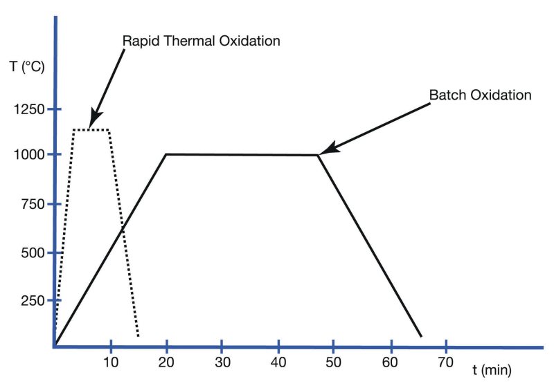
Temperature: 950C° – 1050C°
Gases: Steam
Equipment: Horizontal Furnace
Wet Oxide On Silicon
Our Ultra-Pure Wet Thermal Oxidation process is designed to insure that you receive the highest quality films. Prior to thermal oxidation
all wafers will receive a pre-furnace clean.
Dry Oxide On Silicon
Our ultra-pure Dry Oxidation process is available for those applications requireing thinner oxides, and is designed to ensure that you
receive the highest quality film.
Dry Chlorinated Thermal Oxidation
Our Dry Chlorinated Thermal Oxidation is recommended for use in MOS and other active device fabrication processes. Using Dry Cholorinated Thermal Oxide can help your devices to perform to its highest potential by eliminating metal ions.
Thermal Oxide Calculator
Other Specs Thermal Oxide Thickness Available.
chris@universitywafer.com
50.8mm P/B (100)1-10 ohm-cm 280um SSP $ each
With 300nm of Oxide $ each
with 100nm of LPCVD Nitride $ each
100mm N/Ph (100) 1-10 ohm-cm 500um SSP $12.90 each
with 300nm of oxide $ each
with 100nm of LPCVD Nitride $ each
100mm N/As (100) 0.001-0.005 ohm-cm 500um SSP $ each
with 300nm of oxide $ each
with 100nm of LPCVD Nitride $ each
100mm P/B (100) 1-10 ohm-cm 500um SSP $ each
with 300nm of oxide $ each
with 100nm of LPCVD Nitride $ each
100mm P/B (100) 0.001-0.005 ohm-cm 500um SSP $13.90 each
with 300nm of oxide $ each
with 100nm of LPCVD Nitride $ each
100mm P/B (100) 1-20 ohm-cm 1,00um SSP $15.90 each
with 300nm of oxide $ each
with 100nm of LPCVD Nitride $ each
100mm P/B (100) 0.01-0.02 ohm-cm 525um SSP $13.90 each
with 300nm of oxide $ each
with 100nm of LPCVD Nitride $ each
Let Us Know Which Key Word You Use To Find Us And We'll Discount Your Order!
- thermal oxide
- thermal oxide calculator
- thermal oxide thickness
- thermal oxide wafer
- thermal oxide properties
- thermal oxide growth
- thermal oxide furnace
- thermal oxide dielectric constant
- thermal oxide growth calculator
- silicon wafer thermal oxide
- thermal oxide wafer
- thermal oxide si wafer
- thermal oxidation of silicon
- thermal oxidation of silicon wafer
- thermal oxidation calculator
- thermal oxidation unit
- Wet Oxidation
- Dry Oxidation
- Chemical Vapor Deposition (CVD ) Oxide