
Silicon wafers form the foundation of modern electronics, serving as the substrate for virtually all semiconductor devices. Understanding the differences between doped and undoped silicon wafers is important for picking the right material for specific applications. This guide explores the properties, manufacturing methods, and applications of both doped and undoped silicon wafers, providing useful information for researchers, engineers, and industry professionals.
Key Takeaways About Silicon Wafer Doping
- Doped silicon wafers contain intentionally added impurities to modify electrical properties, enabling precise control of semiconductor behavior
- Undoped (intrinsic) silicon wafers are pure silicon with minimal impurities, maintaining natural semiconductor characteristics
- N-type doping uses Group V elements like phosphorus to add free electrons, creating negative charge carriers
- P-type doping uses Group III elements like boron to create electron "holes," functioning as positive charge carriers
- Doping concentration affects resistivity and conductivity, allowing customization from near-insulator to near-metallic properties
- Highly doped wafers are used for resistive heaters, ohmic contacts, and specialized power electronics applications
- Undoped wafers are preferred for certain microelectronic, photovoltaic, and radiation detection applications requiring minimal impurities
- The semiconductor industry continues to evolve with new applications requiring increasingly specialized silicon wafer specifications
- Selection between doped and undoped wafers depends on specific device requirements, processing compatibility, and performance goals
- Advanced manufacturing techniques enable precise control of both doped and undoped silicon properties for cutting-edge applications
Get Your Quote FAST! Buy Online and Start Researching Today
Introduction to Silicon Wafers
Silicon wafers are thin, circular slices of crystalline silicon manufactured through precise processes to meet the exact standards required by the electronics industry. These wafers serve as the foundation for transistors, integrated circuits, and countless electronic devices that power our modern world. At their most basic level, silicon wafers are classified as either doped or undoped, each with distinct properties and applications that determine their suitability for various semiconductor technologies and electronic component manufacturing.
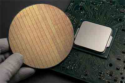
Silicon, as a semiconductor material, has unique electrical properties that position it between conductors and insulators. In its pure form, silicon has limited electrical conductivity, but through a process called doping, we can precisely control its electrical characteristics to achieve specific performance parameters for various electronic applications. The semiconductor industry's remarkable growth shows the importance of silicon wafers, with semiconductor revenues projected to surpass $1 trillion by 2030, driven by increasing demand for computing power, data storage, artificial intelligence, and advanced sensing technologies across virtually every industry sector.
Understanding the differences between doped and undoped silicon wafers is essential for selecting the appropriate material for specific applications in research, development, and manufacturing. Each type offers distinct advantages and is suited to different use cases in the semiconductor industry, from high-performance computing chips to power electronics, photovoltaics, and specialized sensors that enable everything from smartphones to autonomous vehicles and medical devices.
What is Silicon Doping?
Silicon doping is the intentional introduction of impurity atoms into the crystal lattice of pure silicon to modify its electrical properties. This process transforms intrinsic (pure) silicon into extrinsic (doped) silicon with customized electrical characteristics tailored for specific applications in semiconductor devices. Doping represents one of the fundamental innovations that enabled the modern electronics revolution, allowing precise control over semiconductor behavior at the atomic level.
The Doping Process
The doping process involves adding specific impurity atoms to silicon during crystal growth or through post-growth methods. The choice of dopant and its concentration determines the resulting electrical properties of the silicon wafer. Key aspects of the doping process include:
- Dopant selection: Different elements are chosen based on the desired electrical properties, with Group III and Group V elements being the most common dopants due to their compatibility with silicon's crystal structure and their ability to contribute or accept electrons
- Concentration control: Precise control of dopant concentration affects resistivity, with concentrations typically ranging from parts per billion to parts per thousand, allowing for customization across a wide spectrum of electrical behaviors
- Distribution uniformity: Even distribution of dopants throughout the wafer is critical for consistent device performance, requiring sophisticated manufacturing techniques to avoid concentration gradients or clusters
- Thermal processing: Heat treatments activate dopants and repair crystal damage, ensuring proper incorporation of dopant atoms into substitutional lattice positions where they can effectively modify electrical properties
At University Wafer, advanced doping techniques are utilized to create silicon wafers with precise electrical specifications. These doped silicon wafers are used in various semiconductor applications, including power electronics, radiation-hardened electronics, and thermoelectric devices where specific electrical and thermal properties are required for optimal performance.
Types of Doping
Silicon doping primarily falls into two categories: n-type and p-type, each creating distinct electrical characteristics in the semiconductor material.
N-Type Doping
N-type doping involves adding Group V elements (such as phosphorus, arsenic, or antimony) to silicon. These elements have five valence electrons, one more than silicon's four. This extra electron becomes free to move through the crystal lattice, creating negative charge carriers (electrons) and increasing electrical conductivity. The presence of these additional electrons shifts the Fermi level closer to the conduction band, making it easier for electrons to participate in current flow under applied voltage.
P-Type Doping
P-type doping involves adding Group III elements (such as boron, gallium, or indium) to silicon. These elements have three valence electrons, one fewer than silicon's four. This creates "holes" (absence of electrons) in the crystal lattice, which act as positive charge carriers and also increase electrical conductivity. These holes can effectively move through the material as electrons shift to fill them, creating a different mechanism for current flow. P-type doping shifts the Fermi level closer to the valence band of the semiconductor.
The interaction between n-type and p-type regions forms the basis for semiconductor devices like diodes and transistors. The p-n junction created at the boundary between these differently doped regions is fundamental to the operation of most electronic components. When these regions meet, a depletion zone forms where free carriers recombine, creating an electric field that enables the unidirectional flow of current—the basic principle behind diodes, transistors, and most semiconductor devices that power modern electronics.
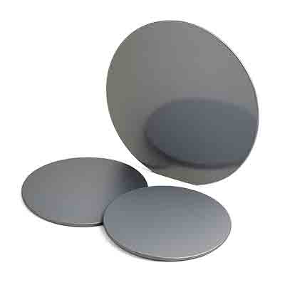
Undoped Silicon Wafers: Properties and Applications
Undoped silicon wafers, also known as intrinsic silicon wafers, contain minimal impurities and maintain the natural semiconductor properties of pure silicon. These wafers serve as the starting material for many semiconductor fabrication processes and have specific applications where pure silicon is advantageous. The absence of intentional dopants results in unique electrical, optical, and physical characteristics that make undoped silicon preferable for certain specialized applications.
Characteristics of Undoped Silicon
Undoped silicon has several distinctive properties that make it valuable for specific applications:
- High resistivity: Intrinsic silicon has significantly higher electrical resistance compared to doped silicon, often exceeding 1,000 ohm-cm, making it suitable for applications where minimal current leakage is critical
- Balanced carrier concentration: Equal numbers of electrons and holes as charge carriers, resulting in the Fermi level positioned near the middle of the bandgap
- Temperature sensitivity: Electrical properties change predictably with temperature, with conductivity increasing exponentially as temperature rises due to thermal generation of electron-hole pairs
- Optical transparency: Better transparency to certain wavelengths of light, particularly in the infrared spectrum, making it valuable for optical and photonic applications
- Uniform crystal structure: Minimal lattice distortion due to absence of dopant atoms, resulting in more consistent mechanical and thermal properties throughout the material
Undoped silicon wafers maintain extremely high purity levels, making them ideal for applications where introducing dopants would interfere with device performance. The uniform crystal structure of undoped silicon also makes it an excellent substrate for subsequent processing steps like thermal oxide deposition, which creates thin layers of SiO₂ on silicon surfaces for semiconductor applications requiring high-quality insulating layers and interfaces.
Applications of Undoped Silicon Wafers
Undoped silicon wafers find applications in various fields where their intrinsic properties provide advantages:
- Microelectronics: Used as starting material for complex integrated circuits where specific doping profiles will be added during device fabrication, providing a clean baseline for precise control of electrical properties
- Photovoltaics: Basis for certain types of solar cells, particularly those requiring high-purity material for maximum efficiency and minimal recombination losses
- Radiation detectors: High-purity silicon for sensitive detection devices where impurities would create noise or false signals, enabling precise measurement of particle energy and trajectory
- MEMS devices: Microelectromechanical systems requiring specific mechanical properties and minimal internal stress, where dopants might alter the desired mechanical characteristics
- Research and development: Testing new device concepts and processes where a well-understood, consistent baseline material is essential for isolating experimental variables
Undoped silicon wafers are manufactured to meet the exact standards required for these applications. They serve as the foundation for transistors, integrated circuits, and solar cells in both research and production environments. The consistent properties of undoped silicon provide researchers and manufacturers with a reliable starting point for developing advanced electronic devices and exploring new semiconductor technologies.
Doped Silicon Wafers: Properties and Applications
Doped silicon wafers have intentionally modified electrical properties through the addition of specific impurity atoms. These wafers form the basis for most semiconductor devices and offer customizable electrical characteristics based on dopant type and concentration. The ability to precisely control electrical behavior through doping has been fundamental to the development of modern electronics, enabling the creation of transistors, diodes, and integrated circuits with specific performance parameters.
Characteristics of Doped Silicon
Doped silicon exhibits several key properties that distinguish it from undoped silicon:
- Controlled resistivity: Dopant concentration precisely determines electrical resistance, allowing customization from near-insulator to near-metallic conductivity depending on application requirements
- Majority carrier type: Either electrons (n-type) or holes (p-type) dominate charge transport, creating predictable electrical behavior under applied voltage
- Enhanced conductivity: Significantly lower resistance compared to intrinsic silicon, enabling efficient current flow in active device regions
- Temperature stability: More stable electrical properties across temperature ranges, with reduced sensitivity to thermal effects compared to undoped silicon
- Fermi level adjustment: Energy level positioning can be tailored for specific device requirements, enabling band engineering for optimized device performance
Doped silicon wafers are manufactured with precise control over dopant type, concentration, and distribution. This allows for the provision of wafers with specific resistivity values tailored to customer requirements for various semiconductor applications, from standard logic devices to specialized power electronics and optoelectronic components.
Applications of Doped Silicon Wafers
Doped silicon wafers are essential components in numerous electronic applications:
- Transistors: The foundation of all modern computing devices, using precisely controlled doping profiles to create field-effect and bipolar junction transistors that amplify and switch electronic signals
- Diodes: Current control and signal rectification devices that rely on the p-n junction formed between differently doped regions
- Integrated circuits: Complex electronic systems on a single chip, combining thousands to billions of transistors with various doping profiles
- Power electronics: High-current and high-voltage applications requiring specialized doping to handle extreme electrical conditions without breakdown
- Photodetectors: Light sensing and conversion to electrical signals, utilizing doped junctions to create the photovoltaic effect
- Thermoelectric devices: Direct conversion between temperature differences and electricity, often using heavily doped silicon to optimize the Seebeck coefficient
Heavily doped silicon wafers are supplied for specialized applications in research and development. These wafers are particularly valuable for manufacturing semiconductors, solar cells, and MEMS devices where specific electrical properties are required. The ability to create regions of varying doping concentration and type within a single wafer enables the complex functionality of modern electronic devices.
Highly Doped vs. Lightly Doped Silicon
The concentration of dopant atoms in silicon creates a spectrum of electrical properties, from lightly doped to highly doped materials. This variation in doping level enables the creation of semiconductor devices with diverse functionalities. The dopant concentration directly affects carrier density, mobility, bandgap narrowing, and other critical electrical parameters that determine device performance and suitability for specific applications.
Lightly Doped Silicon
Lightly doped silicon typically has dopant concentrations in the range of 10¹³ to 10¹⁶ atoms per cubic centimeter. This level of doping creates silicon with moderate conductivity changes while maintaining many of the base properties of silicon. Key characteristics include:
- Moderate resistivity: Typically in the range of 1-100 ohm-cm, providing a balance between conductivity and other semiconductor properties needed for active device regions
- Wider depletion regions: Important for certain transistor designs, allowing for higher breakdown voltages and more gradual junction transitions
- Lower capacitance: Beneficial for high-frequency applications where parasitic capacitance can limit switching speed and signal integrity
- Reduced carrier recombination: Important for solar cell efficiency and other optoelectronic applications where carrier lifetime directly impacts performance
- Less lattice distortion: Maintains more of silicon's mechanical properties, resulting in reduced internal stress and better thermal characteristics
Lightly doped silicon is commonly used in the active regions of many semiconductor devices, particularly where carrier lifetime and mobility are important factors. These regions form the functional core of transistors, photodetectors, and other devices where controlled carrier transport is essential for proper operation.
Highly Doped Silicon
Highly doped or heavily doped silicon contains dopant concentrations exceeding 10¹⁸ atoms per cubic centimeter. This creates material with significantly different electrical properties:
- Very low resistivity: Typically below 0.01 ohm-cm, approaching metallic conductivity levels that enable efficient current flow with minimal resistance losses
- Near-metallic conductivity: Approaches the behavior of conductors, making it suitable for interconnects, contacts, and other applications requiring high current density
- Narrow depletion regions: Used for ohmic contacts where minimal junction effects are desired, enabling efficient transfer of carriers between semiconductor and metal regions
- Higher capacitance: Useful for certain capacitor designs where charge storage density is prioritized over other electrical characteristics
- Degeneracy: Energy bands overlap creating metal-like properties, fundamentally changing the semiconductor behavior toward that of a conductor
Highly-doped silicon wafers are specifically designed for applications requiring low-resistance contacts or specialized electronic components. For example, these wafers are ideal for fabricating resistive heaters using highly-doped silicon substrates with n-type <100> orientation and resistivity in the 0.008-0.015 ohm-cm range. The extreme doping levels create material that behaves almost like a metal while retaining the physical and chemical properties of silicon.
Practical Applications of Doping Concentration Variation
The ability to precisely control doping concentration enables the creation of complex semiconductor devices with regions of varying electrical properties:
- Transistors: Utilize both lightly and heavily doped regions for different functions, with heavily doped source/drain regions for good contacts and lightly doped channel regions for controlled carrier transport
- Solar cells: Employ doping gradients to enhance charge separation, with specific doping profiles creating electric fields that drive photogenerated carriers toward collection contacts
- Power devices: Use doping profiles to control breakdown voltage and current handling, with precisely engineered doping gradients managing electric field distribution under high-voltage conditions
- Integrated circuits: Combine various doping levels to create complete electronic systems, with different transistor types and passive components requiring specific doping profiles
Silicon wafers across the full spectrum of doping concentrations are provided to support these diverse applications in both research and production environments. The ability to create wafers with precisely controlled doping profiles enables the continued advancement of semiconductor technology across virtually every electronic application domain.
Manufacturing Methods for Silicon Wafers
The production of high-quality silicon wafers involves sophisticated manufacturing processes that ensure crystalline perfection, precise dimensions, and controlled electrical properties. Different methods are employed depending on the intended application and required specifications. From initial crystal growth to final polishing and inspection, each step in the manufacturing process must maintain exact standards to produce wafers suitable for semiconductor fabrication.
Crystal Growth Methods
The foundation of silicon wafer manufacturing begins with growing a single crystal of silicon, typically using one of several methods:
- Czochralski (Cz) Method: The most common technique for commercial silicon wafer production, involving pulling a seed crystal from molten silicon while rotating, resulting in a cylindrical ingot. Dopants can be added directly to the melt to create doped silicon. This method produces large-diameter crystals suitable for high-volume manufacturing but typically contains more oxygen impurities from the quartz crucible.
- Float Zone (FZ) Method: Produces higher purity silicon by using a moving molten zone to refine the crystal without a crucible. This method is preferred for high-resistivity applications where impurities must be minimized. FZ silicon typically contains significantly less oxygen and carbon than Cz silicon, making it ideal for high-performance devices and radiation detectors.
- Bridgman Technique: Involves directional solidification of molten silicon in a container, often used for specialized semiconductor materials. The controlled solidification front moves through the melt, creating a single crystal structure with specific properties beneficial for certain applications.
- Gradient Freeze Method: Similar to Bridgman but relies on temperature gradient control rather than physical movement to achieve crystallization. This method can produce crystals with unique dopant distributions and is sometimes used for specialized semiconductor materials.
Advanced crystal growth techniques are utilized to produce silicon ingots with precisely controlled properties, including dopant concentration and distribution. Each method offers different trade-offs between purity, cost, scalability, and crystal quality that must be considered for specific applications.
Wafer Processing Steps
Once the silicon ingot is grown, it undergoes several processing steps to transform it into wafers suitable for semiconductor fabrication:
- Slicing: The cylindrical ingot is cut into thin wafers using diamond wire saws or inner diameter saws. This process must minimize kerf loss (material lost during cutting) while maintaining wafer integrity and precise thickness control.
- Edge rounding: Wafer edges are rounded to prevent chipping and cracking during handling. This step reduces particle generation and improves wafer durability throughout subsequent processing steps.
- Lapping: Mechanical process to flatten the wafer and remove saw marks. This creates a uniform thickness across the wafer and prepares the surface for finer finishing operations.
- Etching: Chemical treatment to remove surface damage and contaminants. This step typically uses acidic or alkaline solutions to dissolve a thin layer of damaged silicon, revealing the pristine crystal structure beneath.
- Polishing: Creates an ultra-flat, mirror-like surface required for semiconductor processing. Chemical-mechanical polishing (CMP) combines chemical etching with mechanical abrasion to achieve nanometer-scale surface smoothness.
- Cleaning: Removes particles and contaminants from the wafer surface. Advanced cleaning protocols using specialized chemicals, ultrasonic agitation, and megasonic energy ensure surfaces meet the strict cleanliness requirements of semiconductor fabrication.
- Inspection: Quality control to ensure wafers meet specifications. Automated optical inspection systems, laser scanning, and other metrology tools verify dimensional accuracy, surface quality, and electrical properties.
For doped wafers, the doping process can occur during initial crystal growth or through subsequent processes like diffusion or ion implantation, depending on the specific requirements. Each processing step must maintain the crystalline integrity and purity of the silicon while achieving the precise dimensions and surface quality needed for semiconductor fabrication.
Post-Growth Doping Methods
While many doped silicon wafers receive their dopants during the crystal growth process, additional doping can be performed after wafer fabrication:
- Thermal diffusion: Exposing wafers to dopant gases at high temperatures to drive impurity atoms into the silicon lattice. This traditional method creates a concentration gradient from the surface inward and is still widely used for certain applications despite being less precise than ion implantation.
- Ion implantation: Accelerating dopant ions to high energies and bombarding the wafer surface, allowing precise control of dopant depth and concentration. This method enables complex doping profiles and is the standard for advanced semiconductor fabrication, offering exceptional control and reproducibility.
- Epitaxial growth: Depositing additional silicon layers with controlled doping on the wafer surface. This technique allows for the creation of abrupt junctions and precisely layered structures with different doping profiles, essential for many advanced device architectures.
- Neutron transmutation doping: Using nuclear reactions to convert silicon atoms to phosphorus, creating uniformly doped n-type silicon. This specialized technique produces exceptionally uniform doping throughout the entire wafer volume, ideal for power devices and other applications requiring homogeneous electrical properties.
These post-growth methods allow for the creation of complex doping profiles and structures required for advanced semiconductor devices. The selection of doping method depends on factors including required precision, depth profile, concentration uniformity, and compatibility with subsequent processing steps.
Comparative Analysis: Doped vs. Undoped Silicon Wafers
When selecting silicon wafers for specific applications, understanding the fundamental differences between doped and undoped options is crucial. This comparison highlights the key distinctions and helps guide appropriate material selection based on device requirements, processing compatibility, and performance goals.
Doped vs. Undoped Silicon Wafers: Key Differences
| Property | Undoped Silicon | Doped Silicon |
|---|---|---|
| Electrical Resistivity | Very high (>1000 ohm-cm) | Controlled (0.001-100 ohm-cm) |
| Charge Carriers | Equal electrons and holes | Predominantly electrons (n-type) or holes (p-type) |
| Temperature Sensitivity | High | Lower, more stable |
| Crystal Purity | Extremely high | Controlled impurities |
| Primary Applications | Radiation detectors, photovoltaics, research | Transistors, integrated circuits, power devices |
| Cost | Higher due to purity requirements | Varies with dopant type and concentration |
Electrical Properties Comparison
The most significant difference between doped and undoped silicon wafers lies in their electrical characteristics:
Conductivity: Undoped silicon has very low conductivity at room temperature, while doped silicon can have conductivity levels that are orders of magnitude higher, depending on dopant concentration. This fundamental difference determines the suitability of the material for active electronic components versus applications requiring high resistivity and minimal current leakage.
Carrier Type: Undoped silicon has equal numbers of electrons and holes as charge carriers, while doped silicon has a predominance of either electrons (n-type) or holes (p-type). This carrier imbalance is essential for creating the rectifying junctions and field effects that enable transistor operation and other semiconductor device functions.
Fermi Level Position: The Fermi level in undoped silicon lies near the middle of the bandgap, while in doped silicon it shifts toward either the conduction band (n-type) or valence band (p-type). This energy level positioning fundamentally affects how the material responds to applied voltage, temperature changes, and optical stimulation.
Temperature Dependence: Undoped silicon shows stronger temperature dependence of electrical properties compared to doped silicon, which can be more stable across temperature ranges. This difference affects device stability and operating temperature range, with doped silicon generally providing more consistent performance across varying environmental conditions.
Depletion Region Formation: When doped silicon of opposite types (p and n) are brought together, a depletion region forms at the junction, creating the basis for diodes and transistors. This phenomenon is absent in undoped silicon, limiting its direct use in active electronic components without additional processing.
Physical Properties Comparison
Beyond electrical differences, doped and undoped silicon wafers also exhibit variations in physical characteristics:
Crystal Structure: Undoped silicon maintains a perfect diamond cubic crystal structure, while dopant atoms in doped silicon create slight lattice distortions. These distortions can affect mechanical properties, thermal expansion, and other physical characteristics, though the effect is typically minimal at standard doping concentrations.
Optical Properties: Doping can affect optical absorption and transmission characteristics, which can be important for optoelectronic applications. Heavily doped silicon typically exhibits increased free-carrier absorption, particularly in the infrared spectrum, while undoped silicon maintains better transparency to certain wavelengths.
Thermal Conductivity: Dopants can influence thermal conductivity, though the effect is typically minor at standard doping levels. At very high doping concentrations, the increased electron scattering can reduce thermal conductivity, which may be relevant for applications involving significant power dissipation.
Mechanical Strength: Heavy doping can sometimes affect mechanical properties, though this is generally not significant at typical doping concentrations. The presence of dopant atoms can create localized strain in the crystal lattice, potentially affecting fracture toughness and other mechanical parameters in extremely heavily doped materials.
Application-Specific Selection Criteria
Choosing between doped and undoped silicon wafers depends on the specific requirements of the application:
- For transistors and integrated circuits: Doped silicon with precise resistivity control is essential. Different regions within these devices require specific doping types and concentrations to create the junctions and field effects that enable electronic functionality.
- For radiation detectors: Ultra-pure undoped silicon provides better sensitivity. The high resistivity minimizes leakage current, while the absence of dopants reduces trapping centers that would compromise detection efficiency.
- For solar cells: Both doped and undoped regions are used in different parts of the cell structure. The p-n junction that enables photovoltaic conversion requires precisely controlled doping, while certain high-efficiency cell designs incorporate minimally doped regions for improved carrier collection.
- For MEMS devices: Selection depends on whether electrical conductivity or mechanical properties are more important. Some MEMS applications prioritize the mechanical characteristics of undoped silicon, while others require the electrical functionality enabled by doping.
- For research applications: The choice depends on the specific parameters being studied. Research into fundamental semiconductor physics, novel device concepts, or material interactions may require either doped or undoped silicon depending on the experimental objectives.
Comprehensive guidance is provided to help customers select the most appropriate silicon wafer type for their specific application requirements. This selection process considers not only the primary functional requirements but also processing compatibility, cost considerations, and long-term reliability factors.
Silicon Wafer Specifications and Quality Metrics
The performance and reliability of semiconductor devices depend heavily on the quality and specifications of the silicon wafers used in their fabrication. Understanding these specifications is essential for selecting the appropriate wafers for specific applications. From dimensional parameters to electrical characteristics and defect metrics, silicon wafer specifications encompass a wide range of properties that must be precisely controlled and measured.
Physical Specifications
Silicon wafers are characterized by several physical parameters that define their dimensions and surface properties:
- Diameter: Standard sizes range from 25.4mm (1 inch) for research applications to 300mm for high-volume manufacturing, with 450mm wafers under development. The industry trend toward larger diameters enables more chips per wafer, improving manufacturing economics for high-volume production.
- Thickness: Typically ranges from 275μm to 775μm, depending on diameter and application requirements. Wafer thickness must balance mechanical stability with processing requirements, with larger diameter wafers generally requiring greater thickness to maintain flatness and resist warping.
- Flatness: Measured as total thickness variation (TTV) and site flatness, critical for photolithography processes. Modern semiconductor lithography requires extreme flatness, often specified to sub-micron levels, to ensure precise pattern transfer across the entire wafer surface.
- Surface Finish: Options include:
- Single-side polished (SSP): One side polished to mirror finish, suitable for applications where only one surface requires processing
- Double-side polished (DSP): Both sides polished, necessary for double-sided processing or backside imaging applications
- Epitaxial layers: Thin crystalline layers grown on the wafer surface with precisely controlled properties
- Thermal oxide coatings: Silicon dioxide layers formed through controlled oxidation for insulation or passivation
- Edge Profile: Defined edge rounding specifications to prevent chipping and particle generation. Edge profile design balances mechanical durability with minimizing the unusable area at the wafer perimeter.
- Crystal Orientation: Common orientations include <100>, <111>, and <110>, each offering different physical and chemical properties. Orientation affects anisotropic etching behavior, surface energy, and certain electrical characteristics that may be relevant for specific device designs.
Electrical Specifications
The electrical properties of silicon wafers are primarily determined by doping characteristics:
- Resistivity: Measured in ohm-cm, ranging from:
- Undoped/intrinsic: >1,000 ohm-cm, suitable for applications requiring minimal free carriers
- Lightly doped: 1-100 ohm-cm, used for many active device regions and general-purpose applications
- Moderately doped: 0.1-1 ohm-cm, common for standard CMOS substrates and many commercial devices
- Heavily doped: <0.1 ohm-cm, used for buried layers, contact regions, and specialized applications
- Dopant Type: P-type (boron, gallium) or N-type (phosphorus, arsenic, antimony), selected based on device design requirements and compatibility with subsequent processing steps
- Dopant Uniformity: Variation in resistivity across the wafer, typically specified as a percentage. Modern device manufacturing requires excellent uniformity to ensure consistent performance across all chips on a wafer.
- Carrier Lifetime: Measure of how long charge carriers remain before recombination, important for devices like solar cells. Longer carrier lifetimes generally indicate higher material quality with fewer recombination centers.
- Oxygen Content: Particularly relevant for Czochralski-grown silicon, affects electrical and mechanical properties. Controlled oxygen concentration can provide beneficial internal gettering of metallic impurities during thermal processing.
Quality Metrics and Defects
Silicon wafer quality is assessed based on the presence and density of various defects:
- Surface Defects:
- Particles: Foreign material on the wafer surface that can interfere with device fabrication
- Scratches: Linear defects that disrupt surface uniformity and can cause device failure
- Haze: Light scattering caused by microscopic surface roughness or contamination
- Edge chips: Small fractures at the wafer perimeter that can generate particles or propagate into larger cracks
- Surface roughness: Nanoscale topography measured by atomic force microscopy or optical techniques
- Bulk Defects:
- Crystal dislocations: Linear defects in the crystal structure that can affect electrical properties
- Stacking faults: Planar defects where the crystal stacking sequence is disrupted
- Swirl defects: Pattern of impurities or vacancies resulting from crystal growth dynamics
- Oxygen precipitates: Clusters of silicon-oxygen compounds formed during thermal processing
- Carbon inclusions: Carbon impurities incorporated during crystal growth
- Contamination:
- Metallic impurities: Transition metals that can create deep-level traps affecting device performance
- Organic contaminants: Carbon-based compounds that can interfere with processing steps
- Ionic contamination: Mobile charged species that can cause instability in oxide layers
- Inspection Methods:
- Optical inspection: Visual examination using specialized lighting to detect surface defects
- Laser scanning: Light scattering techniques to identify particles and surface anomalies
- X-ray topography: Imaging of crystal defects using X-ray diffraction
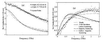
- Electrical testing: Four-point probe and other methods to verify resistivity and other electrical parameters
Detailed specifications are provided for all silicon wafers, and strict quality control processes are maintained to ensure products meet or exceed industry standards for both research and production applications. These specifications are continuously refined as semiconductor technology advances and new applications emerge with increasingly strict requirements.
Advanced Applications and Future Trends
The semiconductor industry continues to evolve rapidly, with silicon wafers remaining at the core of technological innovation. Understanding emerging applications and future trends helps in anticipating the evolving requirements for both doped and undoped silicon wafers. As device architectures become more complex and performance demands increase, silicon wafer technology must advance to meet these challenges while maintaining economic viability.
Emerging Applications
Several cutting-edge applications are driving innovation in silicon wafer technology:
- Quantum Computing: Ultra-pure silicon wafers with precisely placed dopant atoms are being explored for quantum bits (qubits) in silicon-based quantum computers. These applications require unprecedented control over individual dopant atoms and their quantum states, pushing the boundaries of manufacturing precision.
- Silicon Photonics: Integration of optical components on silicon wafers for high-speed data communication, requiring specialized doping profiles and surface treatments. This technology enables optical interconnects that overcome the bandwidth limitations of traditional copper interconnects in high-performance computing and data centers.
- Power Electronics: Wide-bandgap semiconductors and advanced silicon doping techniques for high-voltage, high-efficiency power conversion devices. Silicon carbide and gallium nitride are complementing traditional silicon in this space, but advanced silicon technologies remain competitive for many applications through innovative doping and structural engineering.
- Flexible Electronics: Thin silicon wafers that can bend without breaking, enabling new form factors for electronic devices. These ultra-thin wafers, sometimes less than 50 microns thick, enable silicon-based electronics to be incorporated into curved surfaces, wearable devices, and other non-planar applications.
- Bioelectronics: Silicon-based sensors and interfaces for medical applications, often requiring specialized surface treatments and doping profiles. These devices bridge the gap between electronic systems and biological environments, enabling advanced medical diagnostics, neural interfaces, and implantable therapeutic devices.
- Silicon Anodes for Batteries: Silicon is being explored for advanced battery technologies, particularly for electric vehicles. Silicon's ability to store significantly more lithium ions than traditional graphite anodes makes it promising for high-capacity batteries, though challenges with volume expansion must be addressed.
Industry Trends
The semiconductor industry is experiencing several significant trends that impact silicon wafer requirements:
- Scaling Beyond Moore's Law: As traditional scaling becomes more challenging, new architectures and materials are being explored to continue performance improvements. This includes vertical stacking, novel transistor designs, and heterogeneous integration that place new demands on silicon wafer properties and manufacturing precision.
- 3D Integration: Vertical stacking of silicon dies to increase functionality without increasing chip area, requiring thinner wafers with special handling capabilities. These architectures demand wafers with excellent thickness uniformity, minimal warpage, and compatibility with through-silicon via (TSV) processing.
- Advanced Packaging: Heterogeneous integration of different chip types, often requiring specialized silicon interposers with through-silicon vias (TSVs). These interposers serve as the bridge between different components in advanced multi-chip modules, demanding specific electrical, thermal, and mechanical properties.
- Sustainability Focus: Increasing emphasis on reducing environmental impact through wafer reclamation, energy-efficient processing, and sustainable manufacturing practices. The semiconductor industry is working to reduce water usage, energy consumption, and waste generation while maintaining the exact quality standards required for advanced devices.
Future Developments in Silicon Wafer Technology
Looking ahead, several developments are likely to shape the future of silicon wafer technology:
- Engineered Substrates: Custom-designed silicon wafers with specialized layers, doping profiles, or embedded structures for specific applications. These may include silicon-on-insulator (SOI), silicon-on-nothing (SON), or other advanced substrate technologies that enable novel device architectures and enhanced performance.
- Larger Diameter Wafers: Continued progression toward 450mm wafers for high-volume manufacturing to improve economics. Though this transition has been slower than initially projected, the economic advantages of larger wafers continue to drive research and development in this direction, particularly for high-volume applications.
- Ultra-Thin Wafers: Development of wafers below 100μm thickness for flexible electronics and advanced packaging. These wafers present significant handling challenges but enable new applications where traditional thick silicon would be unsuitable due to rigidity or thermal constraints.
- Defect-Free Production: Advanced crystal growth and processing techniques to eliminate defects that limit device performance. As device dimensions continue to shrink, even nanoscale defects can significantly impact yield and reliability, driving the need for ever-more-perfect silicon crystals.
- Smart Manufacturing: Integration of AI and machine learning for real-time quality control and process optimization in wafer production. These technologies enable adaptive manufacturing processes that can detect and correct variations before they result in defective wafers, improving yield and reducing costs.
Staying at the forefront of these developments is essential, with continuous updates to product offerings to meet the evolving needs of researchers and manufacturers in the semiconductor industry. The ability to anticipate and respond to changing requirements ensures that silicon wafer technology will continue to enable innovation across the electronics ecosystem.
Conclusion
The distinction between doped and undoped silicon wafers represents one of the fundamental choices in semiconductor technology, with far-reaching implications for device performance, manufacturing processes, and application suitability. As this comprehensive analysis demonstrates, each type offers unique advantages that make them indispensable for different aspects of modern electronics manufacturing and research.
Looking toward the future, emerging applications in quantum computing, silicon photonics, flexible electronics, and biomedical devices will continue to challenge traditional wafer specifications and drive innovation in both doped and undoped silicon technologies. The industry's focus on sustainability, advanced packaging, and beyond-Moore's-law scaling will create new requirements for wafer properties, manufacturing processes, and quality metrics.
Success in selecting the appropriate silicon wafer type ultimately depends on understanding the complete system requirements, including electrical specifications, processing compatibility, cost considerations, and long-term reliability goals. As semiconductor technology continues to advance and new applications emerge, the fundamental choice between doped and undoped silicon wafers will remain central to achieving optimal device performance and manufacturing success.