
Could you supply a carrier wafer on suitable the thin wafer and sticky tape together? We need one carrier wafer and sticky tape if we decide to purchase the thin wafer. If you possible, please let me know a price list of carrier wafer and sticky tape.
Carrier Wafers in Stock and Ready to Ship
An electrical engineer requested a quote for the following:
Reference #144132 for specs and pricing.
The following super flat subsrates can be used as carrier wafers:
The substrate holder for other wafers are bonded onto the carrier wafer. Please let us know what carrier wafer spec and quantity we can quote for you!
Get Your Quote FAST! Or, Buy Online and Start Researching Today!
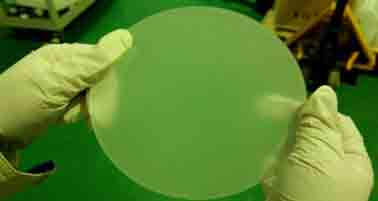
150mm Carrier Wafer
A Orthopaedic biomechanics and mechanobiology researcher requested the following:
I purchased 6" ([100] silicon P/B wafer w/o oxide layer (625um thickness)) from you a year ago. Do you still have this kind of wafers? I just want the 6" wafer with price as low as possible because they are going to be used as the carrier wafer.
Reference #135588 for specs and pricing.
What is a Carrier Wafer?
Vacuum chemical processes and carrier wafer techniques can require the processing and handling of extremely thin semiconductor wafers with extreme surface texture. For instance, carbon nanotube (CNW) and tourmaline mesotherapy applications involve very thin, stiff substrates that must be prepared before any treatments are applied. The application of a carrier wafer minimizes the production costs for many printed circuit devices (PCE) and other solid-state applications (SEDs). But the most cost-effective method of Carrier-Wafer-Based Packaging'is also advantageous: it reduces the total production costs for both CE/SED hybrid devices and solid-state devices.
How to Attach a Sample to a Carrier Wafer
A carrier wafer, also called a sample wafer is glued to a carrier or dummy wafer. This procedure is usually done in a cleanroom environment, but you can practice doing this anywhere!
Use a stable, flat substrate, carrier wafer, and position it under your sample wafer. Then, when your sample wafer has through-holes or vias, or when the process itself will create such holes, for instance during Deep Reactive-Ion Etching (DRIE). This simple process can be seen in the video below and it is optimized to be fast and easy to detach the sample from the carrier after processing.
A carrier wafer is simply a thin film of silicon nitride with a front surface that is etched or imprinted with a substrate. In this case, both the back and the front sides of the carrier wafer are treated with different coating materials to create a thicker, uniform carrier layer than on the substrate that is used in the manufacturing of the rest of the device. The thickness of the carrier layer is based upon several factors such as the thickness and type of coating desired, the operating temperature and humidity, the available substrate that is needed, and the method of manufacturing. A carrier wafer has an electrical and mechanical interplay, such that the mechanical properties of the two layers affect one another, which then affect the overall thickness of the carrier wafer.
A carrier wafer typically consists of two layers. One layer is the flat substrate that is used to transfer electric current or to insulate and cool the electric circuit and the other layer is the metallic backing. The flat substrate has a particular thickness that is predetermined, and the metallic backing is a conductive or non-conductive material that can be made of an assortment of alloys, copper, steel, tin, lead, and aluminum alloys and even titanium. Carrier wafers are an integral part of the assembly of electronic devices, especially those that are flat.
Another method of making the carrier is to use a bonding agent between the metallic backing and the flat substrate. This method is referred to as bonded or brazed Silicon wafers, which are often made to be much thinner than regular silicon wafers, sometimes as much as 0.2 millimeters in some cases. They are sometimes called adapter carrier wafers because they are used where there is not a need for the device to be completely sealed. These types of devices are used in communications applications, for example, where it is not feasible to use a seal so the Silicon will still have mobility. They are also used in heating systems.
In the past, many manufacturers have designed and built their own carrier wafer systems by making a solid carrier onto a solid surface. However, manufacturing and assembly of this kind of wafer was a labor-intensive process that could only be done by the most experienced manufacturers. There is an alternative to making a carrier wafer from scratch, and that is to utilize one of the many HDL based silicone wafer systems available today. Instead of starting with a solid carrier and forming the wafer into its final shape, as is done with traditional silicone wafer systems, an HDL based system makes use of its silicone particles to form a thin layer on the surface of a standard sheet of metal. By using a solid base such as aluminum or tin this type of system can be manufactured quickly and much more economically than is possible using a conventional process.
One of the advantages of HDL based carrier wafers is that the thin silicone layer can be applied to any flat surface, including sheet metal, plastic, wood, and more. This makes them highly versatile, and can be adapted to suit any number of applications. This means that flexible substrate attachment is not limited to a few specific industries. Because of this carrier wafer's versatile nature, it has become one of the leading solutions for addressing a wide variety of very small problems that occur in manufacturing.
A typical application includes a wide range of flat plate devices that are used for heating, cooling, and alignment purposes. Another application includes the manufacturing of thermoset resistors for a wide range of electronic components, where thermal expansion and contraction are unavoidable in many situations. It also can be used for bonding and soldering, although a thin wafer handling method is often preferred for these applications. Other uses include bonding of thin films to a standard sheet metal surface, which can help reduce weight and allow for easier soldering and mounting. And, because it has been designed for use with both hot and cold methods of transfer, it can be adapted to a wide variety of different work pieces, including hand grips, shoulder straps, buttons, and more.
As debonding continues to evolve into an alternative method for bonding, companies that have adapted carrier wafer technology can create a higher level of product quality, efficiency, and safety for a number of different industries. These companies can also provide a more cost effective way to produce a wider range of highly conductive components in a shorter amount of time. These companies can take this technology one step further and incorporate some of the most innovative methods for creating a number of different kinds of devices that require debonding, so that these devices can continue to provide a wide range of performance even when the heat and power sources employed in standard bonding processes are not readily available.
Carrier Wafers Flex Circuit Application
A MEMS researcher requested the following quote:
I want a carrier wafer for flex circuit application. Is there a preferred glass / silicon that is used for this application?
Reference #170394 for specs and pricing.
Electro-Plating Carrier Wafer
I'm just looking for lowest price for electro-plating carrier wafer, just needs to be smooth. resistivity doesn"t matter as it will be metal coated. 100mm, other specs don't matter and quantity 25 wafers.
Reference #180119 for specs and pricing.
Lithium Niobate (LiNbO3) Carrier Wafers for Ultrasound Transducer Application
A start up founder requested the following quote:
My company has an application (ultrasound transducer) where we need to thin lithium niobate wafers (to as this as 22 um) that are bounded to a thick glass (7.4 mm) carrier wafer.
We are looking at 36 degree rotated Y-cut lithium niobate. We are not tied to a specific diameter but are looking at 50 to 100 mm. This is not an optical application so surface finish is not critical.
Reference #221032 for specs and pricing.
Carrier Wafer for DRIE and ICP RIE machine
A Posdoc requested the following quote:
We need a quote for SSP, 100 mm diameter, circle, just want primary flat per industry standard, not sure on thickness - we want to use this as a carrier wafer for small samples in a DRIE and ICP RIE machine.
Reference #228287 for specs and pricing.
Carrier Wafer to Use in Etch and CVD Tools
A Nano Fabrication Lab Manager requested help with the following:
We are in need of a carrier wafer type to use in our Etch and CVD tools since so many researchers have such small samples we will need a robust wafer that would be used often to hold the sample. What do you recommend?
Reference #226802 for specs and pricing.
Sputter Metal onto Carrier Wafer
A System Engineer requested the following quote:
We want to sputter a uniform layer of the metal layer with a thickness around 200 nm (can be Au, Pt or W) on the Si carrier wafer. Then I need to grow a layer of Si on the top of metal layer, the thinness will be around 30 um. We might need 25 4 inch wafers for this application. I was wondering to know whether university wafer can fabricate it or not.
UnviersityWafer, Inc. Quoted
Sputter a uniform layer of the metal layer with a thickness around 200 nm (can be Au, Pt or W) on the 4‘’ Si carrier wafer. Then grow a layer of Si on the top of metal layer, the thinness will be around 30 um.
Reference #261466 for specs and pricing.
Sputtered Cu on Borosilicate Carrier Wafers
A Graduate Research Assistant requested the following quote:
I'd like to polish sputtered Cu on a 100um fused silica substrate + 400um borosilicate carrier wafers. As we performed the lift off process, we found the maximum roughness near the patterns become >1um. I wonder if I could CMP the metal with the surface roughness < 5nm.
Reference # for specs and pricing.
How do Scientists Use Carrier Wafers?
Researcher:
I am developing a temporary bonding process with semiconductor wafers and am in need of a specific type of chemical release carrier wafer, for which I am enquiring as to whether you supply. The carrier wafer requires the following basic specifications: * Size: 3 inch (76.2 mm) * Material: Glass (borosolicate or other) or other material, so long as it is transparent to visible light * Perforation, a.k.a. holes, to allow solvent to go through and attack bonding glue * A primary flat (if there is also secondary flat that is not an issue, but there must at least be a primary flat). The first three criteria have not been an issue in my search but it is the combination with the fourth regarding the primary flat which has been the stumbling block. I look forward to hearing from you whether you have a product(s) which can satisfy my requirements.
Those are the main specs. Otherwise, it should be resistant to common process chemicals like organic solvents such as acetone, isopropanol, and menthane (debonding agent), and be able to withstand temperatures up to 220c. If it's glass or a similar material I am not worried about it being able to withstand my process conditions. Thickness is not really important and could really be anywhere in the range of 300-1000 micron.
The main thing is just having the 4 critieria of a primary flat, the holes for the solvent to go through, it being transparent to visible light so that you can physically see the markers on the other wafer that is bonded to the carrier wafer, and it being 3 inch. Everywhere I have managed to look so far has either:
a) 3 inch, holes, transparent. Or
b) 3 inch, transparent, flat ,.
So if you have all 4 that would be amazing.
I would need a box of 25.
UniversityWafer, Inc. Quoted:
Why Use Silicon Carbide (SiC) Carrier Wafer?
Silicon Carbine (SiC) excellent surface flatness and thermal conductivity make them superior to sapphire and glass. Silicon can easily be bonded onto the SiC.
Why Use Sapphire as a Wafer Carrier?
Sapphire wafer have anisotropic, rhombohedral crystals form of Aluminum Oxide.
UniversityWafer, Inc. sapphire wafers carriers have be fabricated to have multiple holes. The perforations assist in the backside thinning process of Compound Semiconductor wafers for Gallium Arsenide (GaAs), Indium Phosphide (InP), Silicon (Si) and other semiconductors.
Anisotropic single crystal materials thermal expansion is very limited and sapphire’s hardness vary significantly by the substrate’s Ori. But it should not matter much for most uses.
UniversityWafer, Inc and our partners have years of wafer carrier experience
So Why Use Sapphire for your Wafer Carrier?
- Chemicals cannot penetrate Sapphire’s surface.
- Zero-degree sapphire wafer carriers are a good coefficient of thermal expansion match to Gallium Arsenide (GaAs).
- Holed wafer carriers can help improve the debonding process.
What Carrier Wafers are Used in Plasma Etch Systems?
Researcher asks:
What is the cost of the 8” diameter double-side polished sapphire, 1.25mm thick in quantities of 1 and 3. We use these as carriers in a plasma etch system.
UniversityWafer, Inc. Quoted:
Pls see below for the offer on required optical grade 8" 1.25mm thick sapphire wafer
8" C-plane<0001>+/-1° 1.25+/-0.05mm P/P Polished Optical grade
Pure round wafer,without flat cut and semi notch
Pricing : $ depends on quantity
Please reference #262951
Carrier Wafers Available List |
||||||
| Size(inch) | Ori | Thickness | Surface | Remarks | Wafer Grade | Mini Order Qty. |
| 4'' | C-plane<0001>+/-1° | 1.0+/-0.025mm | P/E | Epi polished | Prime | 138pcs |
| 6'' | C-plane<0001>+/-1° | 1.0+/-0.025mm | P/E | Epi polished | Prime | 135pcs |
| 8'' | C-plane<0001>+/-1° | 0.75+/-0.05mm | P/E | Epi polished | Prime | 9pcs |
| C-plane<0001>+/-1° | 1.25+/-0.05mm | P/P | Epi polished | Prime | 16pcs | |
| C-plane<0001>+/-1° | 1.60+/-0.05mm | P/E | Epi polished | Prime | 97pcs | |
| C-plane<0001>+/-1° | 3.00+/-0.05mm | P/P | Epi polished | Prime | 5pcs | |
| 4'' | SiC | 1.0+/-0.025mm | P/P | Epi polished | Prime | 23pcs |
| 4'' | SiC | 2.0+/-0.025mm | P/P | Epi polished | Prime | 1pcs |
| 4~8'' | Silicon | >/=1.0mm | P/E | Epi polished | Prime | 213pcs |
| Notice : | ||||||
| 1. Delivery : 1~6 weeks | ||||||
| 2. Do custom Sapphire wafers upon request from 2'' ~ 12'' | ||||||
| 3. P/E : Single side polished | ||||||
| 4. P/P : Both sides polished | ||||||
| 5. TBD by qty.: Pricing According to the quantity | ||||||
| 6. Wafer Grade: Prime grade ,Optical grade | ||||||
Sapphire Wafer Carrier
Sapphire carrier wafer, 6" any Ori, 0.5 - 1mm thick.

What Are Carrier Wafers?
This article will explore the different types of carrier wafers, including Glass, INSACO and CTE-matched wafers. You can also learn about other types, such as plastic carrier wafers. Listed below are some of the most common types of carrier wafers and the process for using them. In addition, we'll explore the advantages and disadvantages of each. Here's a quick overview of each type.
Glass Carrier Wafers
AGC offers high quality glass carrier wafers and panels to semiconductor manufacturers. Glass substrates are suitable for semiconductor packaging due to their smooth and flat surface. They are used to replace conventional packaging methods. The company's glass panel and wafer products are suitable for various semiconductor processes. These are highly customizable and can be applied to various surfaces. They are available in different thicknesses and sizes. AGC offers both flat and square glass carrier wafers for semiconductor manufacturers.
Corning's glass carrier wafers are ultralow Total Thickness Variations (TTV). This 0.2-um TTV is required for advanced semiconductor manufacturing. Corning's carriers offer better process control, support temporary bonding, and a wide range of thermal expansion coefficients. These features help meet even the most demanding R&D requirements. Glass carrier wafers are scalable to meet the growing demand for semiconductors. However, Corning is focused on providing customers with the best value and flexibility.
INSACO Sapphire Carrier Wafers
INSACO has developed the capabilities to fabricate circular recesses in carrier wafers. These wafers can have one center recess or multiple 2" recesses in one carrier. In order to create these recesses, the carrier must be flat and parallel. It must also be able to withstand high temperatures. In addition, the carrier wafer must have a high thermal expansion factor that matches the material. Handling tools must also be compatible with the carrier wafer material.
INSACO manufactures custom sapphire and ceramic parts and has mastered the productio
n of sapphire carrier wafers. Its facility uses class 100 cleanrooms and offers various services for processing semiconductor wafers, such as laser marking, OD and ID grinding, honing, polishing, and edging. The sapphire carrier wafers that Insaco manufactures meet SEMI silicon and GaAs standard specifications.
CTE Matched Carrier
During standard wafer processing, a CTE matched carrier wafer is placed on a glass or blank substrate. The wafer is held in place by a vacuum chuck, and the carrier wafer can be heated to 250 to 350oC. This method of bonding minimizes interfacial stress by ensuring that the CTE of the carrier and device are equal. While temporary bonding adhesives are typically wildly different, a matched CTE carrier wafer minimizes this stress.
Another method of providing enhanced CTE matching is introducing a thermal expansion matching structure between the IC component and the interposer. This technique involves using a special material called underfill that is drawn into a small spacing. However, this method can be difficult to implement, because the BGA substrate and the interposer are thin and difficult to handle. Nevertheless, the added metal will allow for better CTE matching.
Plastic Carrier Wafers
To protect semiconductors, wafer carriers must meet certain standards to ensure reliable performance. In addition to having a tight tolerance, carrier materials must be static-dispersive, have a wide tolerance window, and resist warpage and distortion. The carrier materials used should also be able to compensate for stress during the molding and setting up processes, and not tilt or rock when resting on an end wall. To ensure reliable and reproducible location of wafers during the transfer process, the carrier material must incorporate compensating features to prevent warpage and distortion.
High-end carrier wafers can be made of glass, quartz, or silicon. These materials provide the ultimate in thermal stability, chemical resistance, and transparency. Glass and quartz are also transparent and easy to clean. They are also recyclable, which helps lower costs and protect the environment. This makes them the ideal material for wafer carriers. But, what makes glass carrier wafers superior to other materials? These materials also have low tolerances and allow the carrier to be reused.
Quartz Carrier Wafers
The benefits of quartz carrier wafers are numerous, including their high thermal conductivity, excellent ortisal trandzmittanse, and low dielectric load. The carrier wafers also feature exceptional UV transparency and are highly resistant to thermal shocks. These benefits make quartz carrier wafers an ideal choice for a wide range of manufacturing equipment. But there are some disadvantages of quartz carrier wafers, as well.
As the name suggests, these carrier wafers are used to hold the semiconductor material. Typically, these carrier plates are made of quartz or silicon. The materials used to manufacture quartz carrier wafers are excellent because they are transparent, acid-resistant, and thermally stable. Moreover, quartz carrier wafers can be cleaned and reused after use, thereby reducing their environmental impact. Quartz carrier wafers can also be used to create specialized packaging and diagnostic tools for semiconductor manufacturing.
Quartz Used in Etching Tool as Carrier Wafer
A researcher fo quantum technology requested the following quote:
I'm interested in Quartz wafers. We will use them in our etching tool as carrier wafer, as they're resistant to fluorine. So we dont care about doping or defect density. We need 4 inch wafers. The crystal Ori doesnt matter for us either. Could you send me a quote for these requirements for 5 to 10 wafers?
Reference #224053 for specs and pricng.
Video: Carrier Wafer Explained
Indium Phosphide Carrier Wafers
A graduate student requested the following quote:
I'm looking at buying 2" thick InP carrier wafers. I want a few (2-3) at least 1mm even 2mm like the one you have in stock, and 10 2" 750micron thick wafers. Since they are all carrier wafers I just need one side polish and thick enough so they can withstand some abuse. I see you have 2mm thick but do you have 10 or so that are about 750 microns thick? I didnt see these on the list. Preferably undoped, with a major flat designated, one side polished, 100 Ori, and desired thickness.
Reference #104574 for specs and pricing.
200mm Silicon Carrier Wafers
A PhD candiate requested a quote for the following:
I am looking for 8" Si wafers to be used as a carrier wafer, so questions you have on your website don't necessarily apply to what I'm needing. The just need to be 8" Si wafer, cheap somewhat like test wafers. We are a university and have non-profit status. Can you email me back with a price quote, please?
Reference #110322 for specs and pricing.
150mm Silicon Carrier Wafers
An engineering student requested the following:
We would like to purchase a 6 inches Silicon carrier wafer. The quality of wafer does not matter. Could you send us a price quote?
Reference #136214 for specs and pricing.
100mm Silicon Carrier Wafers
A postdoctoral student requested the following quote:
I would like to have a quote for 100 pieces of 4" in diameter Si wafers. These will be used as carrier wafer for plasma etching, so doping and Ori do not matter. It will be good if there be no flats. I just want test grade with lowest price.
I am interested in either mechanical or test grade. Could you please tell me about the difference between the two? Is the mechanical grade polished, atomically flat?
Reference #133091 for specs and pricing.
Quartz Carrier Wafer
We are ordering ICP/RIE 4 inch
quartz carrier wafer. It should
be un-doped. No Ori
requirement.
Please send me an official
quotation by email.
Reference #135501 for specs and pricing.
What Silicon Wafer Grade Can Be Used as a Carrier Wafer?
The grade of silicon wafer used as a carrier wafer in semiconductor manufacturing typically depends on the specific requirements of the process and the nature of the substrate being supported. However, for many applications, particularly where high precision is not the primary concern, lower-grade silicon wafers can be effectively used as carrier wafers. These include:
-
Test Grade or Mechanical Grade Wafers: These are often the lowest grade of silicon wafers available. They are typically used for equipment testing, training, or applications where the electronic properties of the wafer are not critical. As carrier wafers, their primary role is mechanical support, so their electronic quality is less important.
I am in need of some 4'' (100 mm) Si wafers. I use them as a carrier wafer, so I would like the cheapest you have available. Please quote the price for 25 wafers. I use them as carrier wafers for processing and would like to have the cheapest available. Last I recall, mechanical grade was the cheapest. Could you please quote the price so I can get the order started?
Reference #130848 for specs and pricing.
-
CZ (Czochralski) Grown Silicon Wafers: While not necessarily the lowest grade, CZ silicon wafers can be less expensive than other types, like Float Zone (FZ) wafers. They are often sufficient for use as carrier wafers.
-
Reclaimed Wafers: These are previously used wafers that have been cleaned and repolished for reuse. While they may not be suitable for high-end device fabrication, they can serve well as carrier wafers.
-
Doped or Undoped Wafers: Depending on the process, both doped and undoped wafers can be used. The doping level may not significantly impact their function as a carrier wafer.
It's important to note that the choice of carrier wafer also depends on factors like the size and thickness compatibility with the thin wafer being processed, as well as the thermal and chemical compatibility with the etching process. In many cases, the lowest grade that meets these physical and compatibility requirements would be sufficient.
Bonding Silicon Wafers With Trench to Carrier Wafer
A posdoctoral researcher requested a quote for the following:
Please provide me a quote for wafer thinning (5 wafer lots). The process will consist of the following steps:
- Bond 2” Si wafer (280 um thick) device side down to a carrier wafer. The devices are partially singulated by a trench that is 10 um deep into the silicon wafer. Carrier wafer can be another 2” wafer but preferably a 6” wafer. A temporary bond (thermal or UV release) should be used to mount the silicon wafer to the carrier wafer. If a UV release bond is used, use a glass carrier wafer
- Thin wafer to 7.5 um +/- 2.5 um which will fully singulate the die but die will be held in place on the carrier wafer
Our Questions and Client's Replies
- Q. How large is the individual device on the 2" wafer?
- A. An array of 15 um (micron) x 15 um devices that are 7 um thick arranged in an xy pattern with a 10 um wide street separating adjacent devices. The devices are partially singulated by a 10 um deep trench in the silicon.
- Q. How thick bonding agent could be allowed?
- Not critical, provided thickness uniformity of the bond line across the wafer is < +/- 0.5 um. Prefer UV release temporary bond that will survive resist develop, resist strip and resist hard bake steps.
- Q. What is width of the 10um-deep trench?
- The total trench depth is 17 um (7 um device thickness + 10 um deep trench in silicon) and the trench width is the width of the street (10 um)
What is required of the surface finish after the thickness is reduce to 7.5+/-2.5um?. Surface finish and flatness should be good enough to perform contact lithography on the silicon wafer surface after thinning. Minimum feature size for lithography is 2 um.
Reference #206464 for specs and pricing.