Borofloat 33 Glass Windows for University Researchers
Get Your BF33 Quote FAST!
Borofloat 33 Glass Wafers for Anondic Bonding
Researchers have used the following BF33 specs to etch microfluidic channels into the glass surface before it is bonded to a
silicon wafer.
BF33 Item #517
100mm 500um DSP Ra <1.5nm Scratch/Dig: 60/40, 1 Flat. Beveled edges
The final device will be used for DNA sequencing experiments
in an academic research lab.
Buy as few as One Borofloat 33 Wafer! We have all diameters in stock and ready to ship!
Borofloat 33 Keywords
Please let us know which keywords below that you used to find us.
- Borosilicate Glass Sheet
- Borofloat 33
- Borofloat Glass
- Borosilicate Glass Wafer
- Pyrex 7740
- Borosilicate Wafers
- Pyrex vs Borosilicate
- Pyrex vs Borosilicate
- Borofloat 33 Glass Price
- Borofloat 33 datasheet
- Borofloat 33 pyrex
- Borofloat 33 cite
- Borofloat 33 properties
- Borofloat 33 index
- Borofloat 33 chemical composition
- Borofloat 33 index refraction
- borosilicate glass sheet suppliers
- schott borofloat 33
- schott borofloat
- borofloat 33 glass
- pyrex wafer
- borosilicate glass sheet price
- 7740 pyrex
- anodic bonding glass to silicon
- pyrex 7740 glass wafer
Schott Borofloat 33 Windows
Our Schott Borofloat 33 wafers have excellent mirror-like surface, a high degree of flatness and an outstanding optical quality. Excellent light transmission and its very weak fluorescence intensities over the entire light spectrum make BOROFLOAT® 33 ideal for a wide range of applications in optics, optoelectronics, photonics and analytical equipment.
Below are just some of the uses for our Borofloat 33 wafers.
- Appliances (interior oven doors, fittings in microwave appliances, window panels for fireplaces)
- Environmental engineering, chemical industry (resistant linings and sight glasses for reaction vessels, microfluidic systems)
- Lighting (protective panels for spotlights and high-power floodlights) Photovoltaics (glass for solar collectors)
- Precision engineering, optics (optical filters and mirrors etc.)
- Medical technology, biotechnology (slides, biochips, titration plates, DNA sequencers, microfluidic systems)
- Semiconductor engineering, electronics, sensors (wafers, display glass) Safety (bulletproof glazing)
Below are just some uses for our Borofloat 33 Wafers sold in small quantities and large.
Borofloat 33 Sensor Applications

![]()
Interdigitated Electrode Arrays
![]()
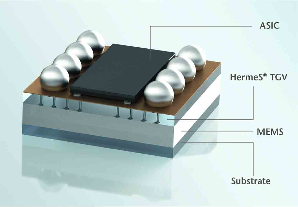
Borofloat 33 substrates used as acceleration, pressure and gyro sensors in automobiles, to switch on light in telecommunications.
Large Area Flat Panel Photon Counting Imaging Detectors for Astronomy and Night Time Sensing.
Borofloat 33 Specs
4" Borofloat 33
Diameter 100 +/-0.3mm
Thickness: 500 +-25um
Also have 175 +/-25um
Double Side Polish
Roughness: <1.5nm (Ra)
TTV: <10um
ground c-shape edge with primary flat acc.to SEMI surface cleanness: scratch-dig 60-40 according to MIL-PRF-13830 clear apeture: diameter 90nm cleanroom packed class 1000 according Fed 209
