Why choose float zone silicon wafers?
Float zone silicon, often abbreviated FZ silicon, is one of the purest forms of silicon available. Compared with silicon grown by the Czochralski (CZ) method, it typically offers lower contamination and is commonly selected for applications that need cleaner electrical behavior and higher resistivity.
 FZ silicon is often used for high-efficiency solar cells, power devices, detectors, infrared work, terahertz optics, RF structures, and advanced research applications. It is also widely chosen where long carrier lifetime and low loss are important.
Quick facts about FZ silicon
- Very high purity with low oxygen contamination relative to conventional CZ silicon
- Available in low, mid, high, very high, and ultra-high resistivity ranges
- Commonly used for detector, RF, THz, infrared, and power-device projects
- Available in multiple diameters, including smaller research wafers through larger production-oriented sizes
Get Your Float Zone Wafer Quote FAST! Or, Buy Online and Start Researching Today!
Unlock high purity and performance
At UniversityWafer.com, we maintain a broad inventory of Float Zone (FZ) silicon wafers for applications where standard CZ silicon may not be the best fit. Sizes range from 1 inch to 8 inch, with select larger options available depending on configuration.
Applications by resistivity range
1. Low Resistivity FZ (< 100 Ω-cm)
Used for high-efficiency energy conversion and standard power switching.
- High-efficiency solar cells
- Power diodes and rectifiers
- Discrete power transistors
- Hall effect sensors
- MEMS actuators

2. Mid-Range High Resistivity (> 1,000 Ω-cm)
The standard range for power handling and improved RF performance.
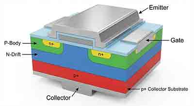
- IGBTs
- RF MEMS switches
- Optical position sensors
- Thyristors
- High-voltage MOSFETs

3. High Resistivity (> 5,000 Ω-cm)
For detector work and lower-loss RF structures.
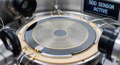
- Silicon drift detectors
- Particle strip detectors
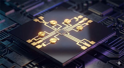
- RFIC substrates
- Deep depletion photodiodes
- Coplanar waveguides

4. Very High Resistivity (> 10,000 Ω-cm)
Useful for microwave and faint-signal detection.
- Microwave monolithic integrated circuits (MMICs)
- High-speed photodetectors
- Avalanche photodiodes
- Passive RF components
- Nuclear radiation detectors

5. Ultra-High Resistivity (> 20,000 Ω-cm)
Often selected for scientific and advanced low-noise applications.
- Terahertz optics and imaging
- Cryogenic physics experiments
- Quantum computing substrate research
- Far-infrared components
- Single-photon detector research

Featured float zone silicon inventory ready to ship
Below is a selection of in-stock Float Zone silicon wafers. For custom requirements or larger quantities, request a quote.
Low Resistivity (< 100 Ω-cm)
| Item # | Diameter | Type | Resistivity (Ω-cm) | Note |
|---|---|---|---|---|
| 12852 | 8" | p-type Si:B | 1-50 | Prime, TTV < 5 μm |
| 11507 | 6" | n-type Si:P | 3-4 | PV FZ, high lifetime |
| B0206 | 6" | p-type Si:B | 1-30 | Prime, back-side lasermark |
| 12535 | 4" | n-type Si:P | 1-5 | PV Prime, MCC > 2,000 μs |
Mid-Range High Resistivity (> 1,000 Ω-cm)
| Item # | Diameter | Type | Resistivity (Ω-cm) | Note |
|---|---|---|---|---|
| 8297 | 8" | p-type Si:B | 2,000-6,000 | Prime, MCC lifetime > 1,000 μs |
| 4982 | 6" | n-type Si:P | > 1,000 | Prime, front-side lasermark |
| 5729 | 5" | p-type Si:B | > 1,000 | Prime, front LM |
| 5744 | 5" | p-type Si:B | > 1,000 | SEMI standard |
| G158 | 4" | n-type Si:P | > 1,000 | Prime, TTV < 2 μm |
High Resistivity (> 5,000 Ω-cm)
| Item # | Diameter | Type | Resistivity (Ω-cm) | Note |
|---|---|---|---|---|
| 10507 | 6" | p-type Si:B | > 8,000 | Prime, 400 μm thick |
| B208 | 6" | n-type Si:P | > 9,500 | Prime, MCC > 6,000 μs |
| E239 | 6" | n-type Si:P | 7,000-8,000 | MCC lifetime = 7,562 μs |
| 12648 | 4" | n-type Si:P | > 5,000 | Prime, 200 μm thick |
| 12489 | 4" | n-type Si:P | 5,000-20,000 | Prime, MCC > 1,000 μs |
Very High Resistivity (> 10,000 Ω-cm)
| Item # | Diameter | Type | Resistivity (Ω-cm) | Note |
|---|---|---|---|---|
| B1417 | 8" | Intrinsic | > 10,000 | Prime, MCC > 1,000 μs |
| 12111 | 6" | Intrinsic | > 10,000 | Prime, TTV < 5 μm |
| A1557 | 4" | Intrinsic | > 10,000 | Prime, TTV < 5 μm |
| 11073 | 4" | p-type Si:B | > 10,000 | Prime, particle count < 20 |
Ultra-High Resistivity (> 20,000 Ω-cm)
| Item # | Diameter | Type | Resistivity (Ω-cm) | Note |
|---|---|---|---|---|
| 10938 | 8" | Intrinsic | > 20,000 | Prime, MCC > 1,000 μs |
| D817 | 6" | Intrinsic | > 65,000 | Prime, notch |
| 12070 | 4" | Intrinsic | > 20,000 | Range up to 189,900 Ω-cm |
| 12030 | 3" | Intrinsic | > 20,000 | Prime, TTV < 5 μm |
Float Zone silicon for infrared spectroscopy
One common request is for double-side polished, lightly doped or intrinsic high-resistivity silicon for infrared spectroscopy measurements. A typical quoted configuration includes 100 mm diameter, approximately 500 μm thickness, and resistivity above 1,000 Ω-cm.
Full general inventory list
| FZ Si Dia | Type / Dopant | Orientation | Resistivity (Ω-cm) | Polish | Thickness (μm) | Comments |
|---|---|---|---|---|---|---|
| 25.4 mm | Undoped | (100) | > 2,000 | SSP | 280 | Intrinsic float zone |
| 50.8 mm | N/Ph | (111) | > 200 | SSP | 200 | 2 flats, back-side alkaline etched |
| 76.2 mm | Undoped | (100) | > 5,000 | SSP | 500 | Undoped float zone |
| 100 mm | P/B | (111) | 40-60 | SSP | 255 | Buy as few as one |
| 150 mm | Undoped | (100) | > 10,000 | DSP | 650 | Hard to find |
| 200 mm | Undoped | (100) | > 1,000 | SSP | 725 | FZ Si TTV < 6 μm |
Frequently asked questions
What makes float zone silicon different from CZ silicon?
Float zone silicon is generally chosen when lower contamination and higher resistivity are more important than the broader availability and lower cost commonly associated with standard CZ-grown material.
Is float zone silicon good for infrared and terahertz applications?
Yes. High-purity, high-resistivity FZ silicon is commonly selected for infrared and terahertz-related work, including optics, windows, lenses, detector research, and measurement setups.
What wafer sizes are available?
This page includes featured inventory ranging from smaller research-friendly diameters through 8-inch wafers, with some larger options available depending on specification.
Can I order a custom thickness or polish?
Yes. Custom diameter, thickness, orientation, polish, and resistivity requests can be submitted through the quote form or the contact page.
