
We want to use the mirror-quality surface of a polished silicon wafer to fabricate laser scanning mirrors. Which silicon wafer specifications would be best for our optical and micromachining process?
Get Your Silicon Laser Mirror Wafer Quote FAST!
UniversityWafer supplies high-quality polished silicon wafers for laser scan mirrors, MEMS beam-steering devices, LiDAR systems, optical scanners, laser engraving, and photonics research.
Not sure which silicon substrate to order? Our team can help you choose the appropriate wafer diameter, thickness, crystal orientation, resistivity, and surface finish for your laser mirror fabrication process.
Researcher Request
Buy as few as one wafer for research, prototyping, or process development. Buy Silicon Wafers Online or submit your specifications below for a fast quotation.
Recommended Silicon Wafer Specifications
- Surface finish: Prime-grade polished or double-side polished
- Crystal orientation: (100), (110), or (111)
- Wafer diameter: 50 mm, 76.2 mm, 100 mm, 150 mm, 200 mm, or custom
- Thickness: Standard or custom thickness for stiffness and low mass
- Resistivity: Standard, low-resistivity, or high-resistivity silicon
- Doping: P-type, N-type, or intrinsic silicon
- Surface quality: Low roughness, low bow, low warp, and controlled TTV
Common Processing Requirements
- Photolithography and patterning
- Deep reactive ion etching (DRIE)
- Wet anisotropic silicon etching
- Thin-film reflective coatings
- Backside etching and release
- Wafer bonding
- MEMS actuator fabrication
- Dicing into custom mirror shapes
Silicon Wafers for Optical Research
Polished silicon substrates are commonly selected for research involving MEMS scanning mirrors, optical beam steering, LiDAR, laser ranging, 3D imaging, miniature projectors, and optical sensing systems. We can supply full wafers, diced pieces, and small quantities for early-stage development.
What Is a Laser Scan Mirror?
A laser scan mirror is an optical component used to redirect and move a laser beam across a surface, object, or three-dimensional space. The mirror may rotate, tilt, oscillate, or move resonantly to control the direction and position of the reflected beam.
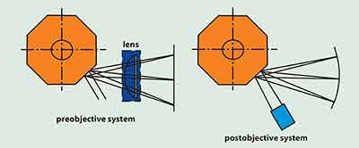
Depending on the optical system, laser scanning mirrors may be flat, curved, parabolic, or fabricated as miniature MEMS scanning mirrors. They are widely used in LiDAR, laser engraving, laser cutting, 3D printing, barcode scanning, medical imaging, projection systems, and optical inspection equipment.
Why Use Silicon for Laser Scan Mirrors?
Polished silicon wafers are attractive substrates for laser scan mirror fabrication because silicon combines excellent mechanical strength, low mass, dimensional stability, semiconductor-processing compatibility, and a highly polished surface. These properties make silicon especially useful for compact optical scanners and microelectromechanical systems.
Silicon scan mirrors can also be fabricated using established semiconductor processes such as photolithography, wet etching, deep reactive ion etching (DRIE), thin-film deposition, and wafer bonding. This allows researchers to integrate mirrors, actuators, sensors, and control structures on the same substrate.
Important Silicon Wafer Properties
The performance of a silicon laser mirror depends on selecting the correct wafer specifications. Researchers should consider surface finish, wafer thickness, crystal orientation, resistivity, flatness, and compatibility with reflective coatings.
- Surface roughness: A smooth, prime-grade surface helps reduce optical scattering and improves reflected beam quality.
- Wafer flatness: Low bow, warp, and total thickness variation help maintain accurate mirror geometry.
- Thickness: Thinner substrates reduce mass and moment of inertia, while thicker substrates provide greater mechanical rigidity.
- Crystal orientation: Common options include (100), (110), and (111), depending on the micromachining process.
- Surface finish: Single-side polished or double-side polished silicon may be selected according to fabrication and alignment requirements.
- Resistivity and doping: Electrical properties may be important when the mirror includes electrostatic, piezoelectric, or electromagnetic actuation.
Reflective Coatings for Silicon Mirrors
Bare silicon does not provide maximum reflectivity at every laser wavelength. For many optical systems, the polished silicon surface is coated with a reflective metal or dielectric film selected for the operating wavelength and laser power.
- Aluminum: Common for ultraviolet, visible, and infrared optical systems.
- Gold: Frequently used for infrared laser scanning and thermal imaging.
- Silver: Offers high reflectivity across much of the visible and near-infrared spectrum.
- Dielectric coatings: Can provide very high reflectivity over a specific wavelength range.
The coating process must maintain good adhesion, low residual stress, and uniform thickness so that the silicon mirror does not bend or distort.
Low Moment of Inertia and Fast Scanning
High-speed laser scanning requires a mirror with a low moment of inertia. Reducing the mirror mass allows the actuator to move the optical surface more rapidly while using less power. Silicon is well suited to this requirement because it can be precisely micromachined into thin, lightweight mirror structures.
Mirror dimensions, support geometry, actuator design, and resonant frequency must be carefully balanced. Excessive vibration, mechanical stress, or deformation can reduce positioning accuracy and distort the reflected beam.
MEMS Laser Scanning Mirrors
A MEMS laser scanning mirror is a miniature movable mirror fabricated using semiconductor manufacturing techniques. MEMS mirrors may provide one-axis or two-axis beam steering and can be driven using electrostatic, electromagnetic, piezoelectric, or thermal actuators.
Silicon MEMS mirrors are used in compact LiDAR systems, augmented-reality displays, medical imaging instruments, miniature projectors, optical communication systems, and portable 3D scanners.
Laser Scan Mirrors for LiDAR
In a LiDAR system, the scan mirror directs laser pulses across the surrounding environment. The reflected light is collected by a detector and used to calculate distance, position, and three-dimensional shape.
Accurate beam steering is especially important in autonomous vehicles, robotics, surveying, industrial mapping, and navigation systems. Mirror flatness, actuator repeatability, scanning angle, resonant frequency, and coating reflectivity all influence LiDAR performance.
Thermal Stability and Laser Damage
Laser scan mirrors may be exposed to concentrated optical power, rapid movement, and repeated temperature changes. The substrate and coating must therefore tolerate the expected laser intensity without warping, cracking, delaminating, or losing reflectivity.
For higher-power systems, researchers should evaluate laser damage threshold, heat dissipation, coating absorption, mirror thickness, and mounting conditions. A stable silicon substrate can help preserve beam accuracy during long-term operation.
Common Laser Scan Mirror Applications
- LiDAR and laser ranging
- 3D scanning and mapping
- Laser cutting and engraving
- Additive manufacturing and 3D printing
- Barcode and document scanning
- Medical imaging and diagnostics
- Optical coherence tomography
- Projection and display systems
- Industrial inspection
- Robotics and autonomous navigation
Choosing a Silicon Wafer for Mirror Fabrication
When requesting a silicon wafer for laser scan mirror research, provide the desired wafer diameter, thickness, crystal orientation, surface finish, resistivity, coating requirements, and quantity. It is also helpful to specify whether the wafer will be used for MEMS processing, DRIE, wafer bonding, backside etching, or thin-film deposition.
UniversityWafer can supply polished silicon wafers, double-side polished wafers, custom thicknesses, diced pieces, and research quantities for laser scanning mirror development and optical beam-steering applications.