
"We are interested in Mg-doped GaN epilayers (5-6 μm thick) on patterned sapphire substrates. We would like information regarding available sapphire patterns and the structural quality of the GaN epilayers, including resistivity, dislocation density, and surface roughness. Our primary interest is in cone patterns having a width of 2.5 μm, a height of 1.7 μm, and a separation distance of 3 μm."
Mg-Doped GaN Wafers for Research and Device Fabrication
UniversityWafer, Inc. supplies custom magnesium-doped (Mg-doped) wafers for research in LEDs, laser diodes, power electronics, sensors, and optoelectronics. Available materials include Mg-doped GaN on sapphire, MgZnO films, and other compound semiconductor substrates with custom specifications.
Researchers can request custom epilayer thicknesses, patterned sapphire substrates, orientations, diameters, and surface finishes to meet demanding semiconductor fabrication requirements.
Mg-Doped GaN Epilayers on Patterned Sapphire
A scientist from a major university requested the following:
Reference #268068 for specifications and pricing.
Get Your Quote FAST! Or, Buy Online and start researching today.
What Is Magnesium-Doped Zinc Oxide (MgZnO)?
Magnesium-doped zinc oxide (MgZnO) is a transparent conductive oxide (TCO) material formed by incorporating magnesium into ZnO. MgZnO combines excellent optical transparency with electrical conductivity, making it useful for advanced semiconductor and optoelectronic devices.
MgZnO materials are widely studied for ultraviolet photodetectors, transparent electronics, chemical sensors, and photovoltaic applications because of their tunable bandgap and excellent electrical properties.
Applications of MgZnO Materials
MgZnO is commonly used in:
- Transparent electrodes
- LCD and touch-screen displays
- Solar cells and photovoltaic devices
- Photodetectors and UV sensors
- Flexible electronics
- Optoelectronic devices
- Chemical and gas sensors
- Transparent conductive films
- High-temperature semiconductor research
Researchers continue to investigate MgZnO for next-generation electronic devices due to its high transparency, low cost, and compatibility with semiconductor manufacturing processes.
What are Magnesium (Mg) Doped Wafers?
Magnesium (Mg) doped wafers are semiconductor substrates intentionally doped with magnesium atoms to create p-type semiconductor materials. Mg doping is widely used in GaN, ZnO, and other compound semiconductors to improve electrical conductivity and optimize carrier concentration for advanced electronic and optoelectronic devices.
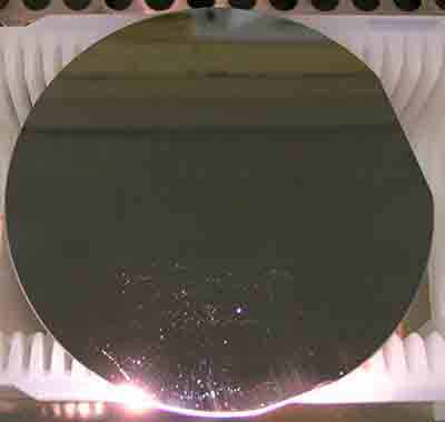
Mg-doped wafers are commonly used in LED fabrication, laser diodes, solar cells, chemical sensors, photodetectors, and power electronics. Their ability to provide stable p-type conductivity makes them essential for modern semiconductor research and production.
Mg-Doped GaN Epilayers on Sapphire
Researchers frequently request Mg-doped GaN epilayers grown on patterned sapphire substrates for high-efficiency optoelectronic devices. These structures are widely used in:
- Blue and UV LEDs
- Laser diodes
- Photonic devices
- High-electron mobility transistors (HEMTs)
- Power electronics
- RF devices
Typical specifications include epilayer thicknesses of 5-6 μm with custom sapphire patterns, low surface roughness, and controlled dislocation densities.
What is MgZnO?
Magnesium-doped zinc oxide (MgZnO) is a transparent conductive oxide that combines the electrical properties of ZnO with the bandgap engineering capabilities of magnesium. MgZnO materials are widely studied for ultraviolet photodetectors, transparent electronics, chemical sensors, and photovoltaic applications.
MgZnO films exhibit excellent optical transparency, high sensitivity, and improved electrical characteristics after thermal annealing, making them attractive for next-generation semiconductor devices.
Applications of Magnesium Doped Wafers
Magnesium doped semiconductor wafers are used throughout the microelectronics and photonics industries. Common applications include:
- Light-emitting diodes (LEDs)
- Laser diodes
- Solar cells and photovoltaics
- Transistors and integrated circuits
- Chemical and pH sensors
- Ion-sensing devices
- Photodetectors
- Optoelectronic devices
- Power semiconductor devices
- Flexible electronics
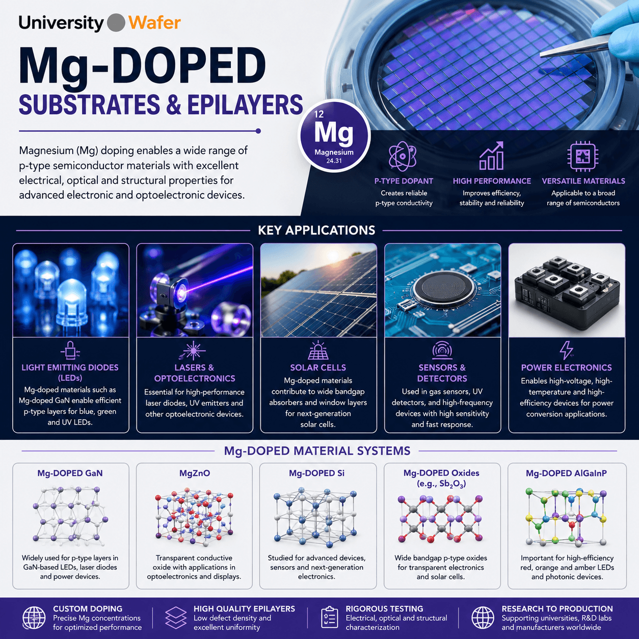
Advantages of Magnesium Doping
Mg doping offers several benefits for semiconductor devices, including:
- Stable p-type conductivity
- Improved carrier concentration control
- Enhanced optical performance
- Reduced defect density
- Higher device efficiency
- Better thermal stability
- Compatibility with GaN and ZnO materials
Custom Mg-Doped Wafers for Research
UniversityWafer, Inc. supplies custom magnesium doped wafers and compound semiconductor substrates for universities, government laboratories, and industrial R&D programs. Available materials include Mg-doped GaN, MgZnO, and other specialized semiconductor structures with custom thicknesses, diameters, orientations, and surface finishes.