We Sell NAND Wafers for Research & Production
NAND Wafers in Stock
We have the following NAND wafers to offer: - Samsung 512Gb, V5 NAND Wafer - 12” V5 NAND Wafer (512Gb) - Good Die Yield : about 93% - 12inch Wafer Net Die : 670ea - Map Data -
Reference #r269943 for pricing
Get Your Quote FAST!
What are Some NAND Wafer Research Terms?
Below are just some key terms associated with NAND wafers.
- flash chip
- hynixs memory
- memory fabrication
- flash wafers
- wafer warping
- flash memory
- nand technologies
- nand memory
- integrated flash
- flash controller
- memory chips
- nand wafers
- wafer fabrication
- microsd card
- flash architecture
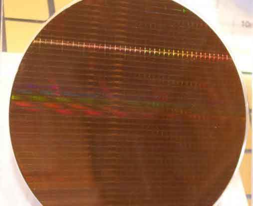
What Does a NAND Wafer Look Like?
Below is a typical 300mm NAND Wafer.

What are NAND Wafers?
NAND wafers are the basic building blocks of flash memory. They are thin, fast, and capable of storing  massive amounts of data. However, due to their fragile nature, data recovery from NAND storage is difficult. Data recovery requires specialized and delicate equipment. NAND wafers are arrayed or die stacked in order to achieve higher capacities.
NAND flash memory is a type of non-volatile storage technology
NAND flash memory is a type of technology that uses electrically conductive materials to store data. It comes in two different forms: consumer grade and industrial grade. Both types have significant advantages and disadvantages. Consumer grade NAND is faster and cheaper than industrial grade NAND, but it is less durable.
NAND flash memory does not need any additional power source to retain data. Its unique structure allows it to be smaller than other forms of storage. It uses tiny memory chips that are about the size of a fingernail. The chips allow for huge amounts of data to be stored.
Although flash memory is non-volatile, it has a finite number of program-and-erase (P/E) cycles. Most commercially available flash products are rated for up to 100,000 P/E cycles, but over that number, the memory cells begin to break down and lose their storage integrity. To compensate for this limitation, manufacturers have developed industrial SSDs that are rated for 1,000,000 P/E cycles.
Consumer devices containing NAND flash memory have millions of memory cells that are stacked horizontally and vertically. They can work in temperatures as low as -40degC and as high as 85degC. However, these devices are more expensive to manufacture than traditional hard drives.
NAND flash memory is used in smartphones, tablets, and digital televisions. Because of its non-volatility, it can store data even if a power source is removed. This makes it ideal for storing important data. As more devices become digital, the need for non-volatile memory will increase.
NAND flash memory was first introduced by Toshiba in 1989. Its architecture is similar to a block device. A block consists of a number of interconnected NAND cells connected by bitlines. A block consists of 512, 2,048, or 4,096 bytes. A few bytes are used for error-correction code checksums.
NAND flash memory can be programmed to store any kind of data. This type of memory requires less power than NOR flash. But it is limited in lifespan and capacity.
It requires a cell to be written to
NAND wafers are semiconductor chips that store information in a massive quantity. Each cell has a binary input and output and is organized into a two-dimensional matrix. Writing to one cell will change information on the adjacent cell. When writing to another cell, 'old' data is marked for deletion and 'good' data is moved elsewhere. When the 'good' data is moved, the entire block is erased.
It is arrayed or die stacked to achieve higher capacities
Many modern computer memory devices use a combination of multiple flash chips in arrayed or die-stacked configurations to achieve higher storage capacities. NAND and NOR flash chip manufacturers have been using this method for many years to increase storage capacity within an IC package. The process is typically used in consumer electronics.
NAND flash memory is a solid-state mass memory element that is available in a variety of forms, including single and multi-level cells. The various types are used for a variety of applications and optimizations. In many cases, a NAND array is composed of several thin dies stacked together inside a module.
In recent years, manufacturers have shifted to 3D NAND. The new technology can store more than 1 TB of data on a 2.5-inch form factor. This technology is more expensive than planar NAND but provides higher storage capacities.
The number of layers in a NAND array is almost limitless. The challenge with this process is maintaining uniform thickness and spacing among the layers. As layers are added, stress builds up and can lead to distortion of patterns and warping of the wafer. Also, the process requires more steps and is more expensive than a single-die structure.
Three-dimensional NAND (or 3D NAND) chips differ from their planar counterparts in that they are stacked vertically. They can achieve greater capacities without sacrificing durability, while reducing power consumption and cost per gigabyte.
