
“I want to order 50 units of Borofloat 33 glass (ID: 517) and 25 units of single-crystal quartz (ID: 1210). The Borofloat 33 glass will be used for anodic bonding with silicon wafers. The quartz will be used in a sacrificial-layer etching process to fabricate nanochannels.”
Request Wafers for Nanochannel Fabrication
UniversityWafer supplies polished silicon, Borofloat 33 glass, fused silica and single-crystal quartz wafers for nanofluidic research. Choose a material to match your patterning, bonding, optical access and surface-chemistry requirements. The channels are fabricated by the researcher's process; ordering a substrate alone does not include patterned nanochannels.
A Researcher's Substrate Request
Reference #209714 when requesting specifications and a quote. View Borofloat 33 item #517 or browse single-crystal quartz. Item #1210 is listed as ST-cut quartz; verify the required crystal cut and processing compatibility before ordering.
Include These Specifications
- Substrate material, wafer diameter, thickness and quantity.
- Surface finish, flatness, roughness and cleanliness requirements.
- Target channel width/depth, patterning method and cover-wafer material.
- Bonding method, surface treatment and operating solution.
- Crystal cut if selecting single-crystal quartz.
Get Your Nanochannel Substrate Quote FAST! Share your wafer specifications and fabrication plan below.
What Are Nanochannels?
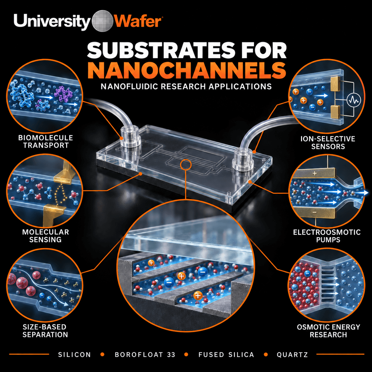
Nanochannels are fluid passages with at least one dimension on the nanometer scale. They can be patterned into a substrate and sealed with a cover layer to make a nanofluidic device. Their behavior depends on channel geometry, surface properties and the liquid or electrolyte used in the experiment.
Choosing a Substrate for Nanochannels
- Silicon: compatible with established lithography and etching methods; an oxide or other surface layer may be added when electrical insulation or different surface chemistry is needed.
- Borofloat 33 glass: provides optical access and can be a cover wafer for anodic bonding to silicon when the materials and bonding process are suitable.
- Fused silica: a transparent, amorphous SiO₂ substrate for optical access and selected chemical environments; use a bonding method suited to fused silica.
- Single-crystal quartz: a crystalline SiO₂ option when the crystal orientation or its optical and piezoelectric properties matter. Specify the cut and check etching behavior.
Fabrication and Sealing Considerations
A nanochannel process may pattern features using electron-beam lithography or another suitable technique, etch or form the channel in the selected material, then seal it with a compatible cover wafer. The usable process depends on channel dimensions, material, mask, etch chemistry and bonding temperature. A bond that works for borosilicate glass and silicon should not be assumed to work for every glass or quartz substrate.
Surface Charge and Ion Transport
Charged channel walls can form an electrical double layer in an electrolyte. As channel dimensions approach relevant electrostatic length scales, surface charge can have a strong influence on ion transport and electroosmotic flow. The effect depends on ionic strength, pH, wall chemistry and geometry; it is not an inherent property of every nanochannel.
Research Applications
Researchers study nanochannels for biomolecule transport, sensing, size-based separation, ionic selectivity and osmotic-energy concepts. The substrate supplies a surface and fabrication platform; device performance also depends on channel patterning, sealing, surface functionalization and the measurement setup.