Substrates for Quantum Materials Research
Quantum materials research often requires substrates with carefully controlled
crystal structure, surface quality, electrical properties, optical transmission,
thermal stability, and thickness. UniversityWafer supplies substrate options for
experiments involving thin films, spectroscopy, low-dimensional materials,
transport measurements, photonics, and quantum-device development.
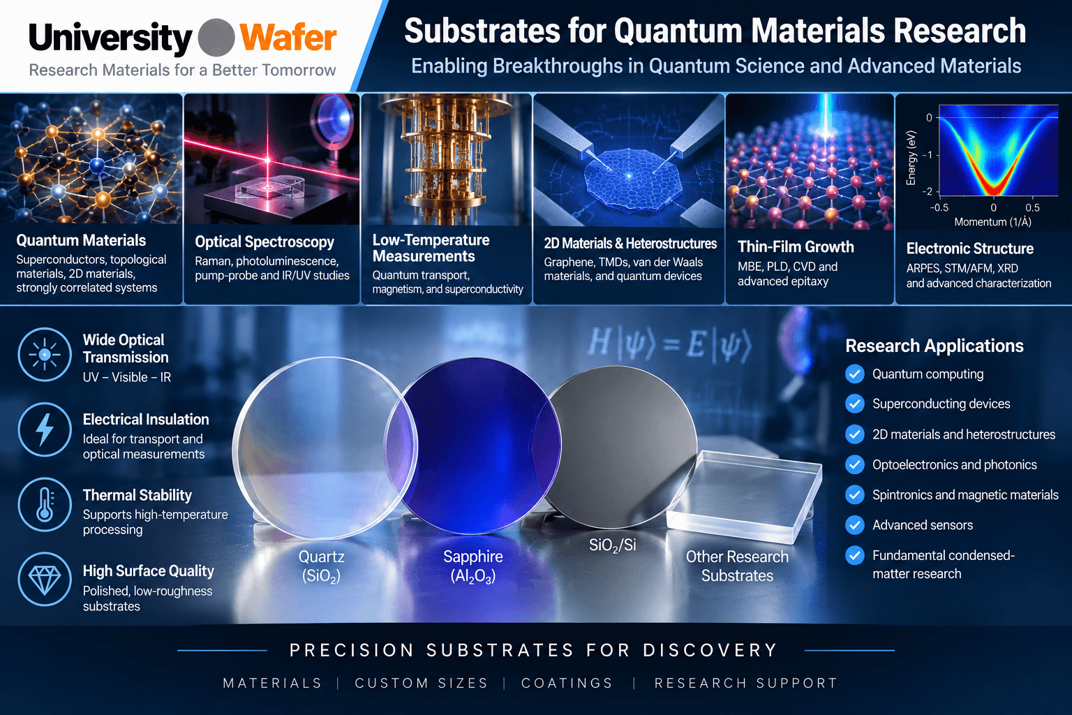
Common substrate choices include
single-crystal quartz
,
sapphire
,
and
SiO2/Si wafers
.
The best choice depends on whether the experiment requires electrical isolation,
optical access, a crystalline surface, thin-film compatibility, or device fabrication.
Example Quantum Materials Research Request
A Materials Science and Engineering Ph.D. researcher requested substrates for
experiments investigating light-driven phenomena in quantum-engineered materials
and their potential use in photonic, polaritonic, optoelectronic, and quantum devices.
Requested Substrates
-
Single-Crystal Quartz
for preliminary optical and materials evaluation.
-
Sapphire
for comparison with quartz in optical and thin-film experiments.
-
SiO2/Si
for thin-film, 2D-material, and device-fabrication research.
The researcher also requested information about
optical transmission from the ultraviolet through the infrared.
Transmission depends on the substrate material, crystal grade, orientation,
thickness, surface finish, and wavelength range.
Reference #278231 for example specifications and pricing.
Get Your Quantum Materials Substrate Quote FAST!
Or,
Buy Wafers Online
and Start Your Research Today!
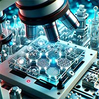
How Are Quantum Materials Made and Studied?
Quantum-material research can involve
bulk crystal growth, thin-film deposition, exfoliation, transfer,
lithography, spectroscopy, microscopy, electrical measurements,
magnetic measurements, and theoretical modeling.
The exact equipment depends on the material and the physical phenomenon being investigated.
Thin-Film & Material Synthesis
Researchers use different growth techniques depending on composition,
crystal structure, required film quality, and substrate compatibility.
-
Furnaces:
used for thermal processing, solid-state reactions, crystal preparation,
annealing, and selected synthesis routes.
-
Molecular Beam Epitaxy (MBE):
enables highly controlled deposition of thin crystalline layers under
ultra-high-vacuum conditions.
-
Pulsed Laser Deposition (PLD):
transfers material from a solid target to a substrate and is widely used
for research on complex oxide and other thin-film systems.
-
Chemical Vapor Deposition (CVD):
can be used to grow selected semiconductors, two-dimensional materials,
and other functional thin films.
Crystal Structure Characterization
Understanding crystal orientation, phase, lattice spacing, and structural
disorder is essential because these features can strongly influence quantum behavior.
-
X-Ray Diffraction (XRD)
– identifies crystalline phases, lattice parameters, orientation, and structural quality.
-
Transmission Electron Microscopy (TEM)
– provides high-resolution information about interfaces, defects, and atomic structure.
-
Scanning Electron Microscopy (SEM)
– examines surface morphology, microstructure, and device features.
Atomic & Electronic Structure
-
Scanning Tunneling Microscopy (STM)
– probes conductive surfaces with atomic-scale spatial resolution and can
provide information about the local electronic density of states.
-
Atomic Force Microscopy (AFM)
– measures surface topography, roughness, steps, and nanoscale morphology
on conducting or insulating samples.
-
Angle-Resolved Photoemission Spectroscopy (ARPES)
– maps the electronic band structure by measuring the energy and momentum
of emitted photoelectrons.
Optical & Vibrational Spectroscopy
Optical techniques are particularly useful for studying excitations,
lattice vibrations, electronic transitions, and light-driven phenomena
in quantum materials.
-
Raman Spectroscopy:
probes vibrational modes, strain, crystal symmetry, defects, and phase changes.
-
Fourier-Transform Infrared Spectroscopy (FTIR):
measures wavelength-dependent infrared absorption, transmission, or reflection.
-
Optical Spectroscopy:
investigates absorption, reflection, emission, and other light-matter interactions.
-
Pump-Probe Spectroscopy:
uses time-separated optical pulses to study ultrafast carrier,
excitonic, lattice, and other transient phenomena.
Electrical Transport Measurements
Electrical measurements reveal how charge carriers move through a material
as temperature, magnetic field, electric field, pressure, or other conditions change.
-
Resistivity Measurements:
track electrical transport and can reveal phase transitions.
-
Hall Effect Measurements:
provide information about carrier type, carrier density, and mobility
under appropriate transport models.
-
Four-Point Probe Measurements:
reduce the influence of contact resistance when measuring sheet resistance
or resistivity.
Magnetic Characterization
-
SQUID Magnetometry:
provides highly sensitive measurements of magnetic moment and magnetic response.
-
Magnetotransport:
studies how electrical resistance and other transport properties change
with applied magnetic field.
-
Nuclear Magnetic Resonance (NMR):
can probe local magnetic and electronic environments within suitable materials.
Low-Temperature Research
Many quantum phenomena become easier to observe when thermal energy is reduced.
Cryogenic systems can therefore be essential for studying superconductivity,
quantum transport, magnetic states, and other low-temperature phenomena.
-
Cryostats:
provide controlled low-temperature environments for optical,
electrical, and magnetic measurements.
-
Dilution Refrigerators:
enable experiments at millikelvin temperatures for selected
quantum-material and quantum-device studies.
High-Pressure Experiments
Diamond anvil cells can generate extremely high pressures,
allowing researchers to modify atomic spacing and investigate pressure-induced
changes in electronic, magnetic, and structural phases.
Computational Modeling
Experimental quantum-material research is often combined with computational
approaches such as electronic-structure calculations, many-body models,
molecular simulations, and other numerical methods.
High-performance computing can help researchers compare theoretical predictions
with measurements and investigate properties that may be difficult to isolate experimentally.
Choosing Substrates for Quantum Materials Experiments
The best substrate depends on the measurement and fabrication process.
Researchers should consider:
- Optical transmission range for spectroscopy and photonics.
- Electrical conductivity or insulation for transport measurements.
- Crystal orientation and lattice structure for thin-film growth.
- Surface roughness and cleanliness for interfaces and 2D materials.
- Thermal expansion and process temperature for deposition and annealing.
- Thickness and flatness for lithography and device processing.
- Dielectric environment when substrate screening may influence the material under study.
UniversityWafer can help researchers select quartz, sapphire,
SiO2/Si, silicon, and other research substrates
based on the experimental requirements of quantum-material studies.
What Are Quantum Materials?
Quantum materials are materials whose electronic, magnetic,
optical, or structural properties are strongly influenced by quantum-mechanical
effects and collective interactions between electrons, spins, orbitals, and
the crystal lattice.
Unlike conventional materials whose behavior can often be described using
relatively simple electronic models, many quantum materials exhibit
emergent behavior. Their macroscopic properties arise from
interactions among large numbers of particles and may include superconductivity,
unusual magnetic ordering, topological electronic states, or strongly
correlated electron behavior.
Important Classes of Quantum Materials
-
Superconductors – materials that can enter a state with
zero electrical resistance and expulsion of magnetic flux below a critical temperature.
-
Topological materials – materials whose electronic band
structure can support unusual surface, edge, or bulk states associated
with topology and symmetry.
-
Strongly correlated materials – systems in which
electron-electron interactions are too important to treat the electrons
as nearly independent particles.
-
Quantum magnetic materials – materials in which spin,
magnetic frustration, exchange interactions, or quantum fluctuations
produce unusual magnetic states.
-
Two-dimensional materials – atomically thin systems such
as graphene and transition-metal dichalcogenides that can exhibit strongly
thickness-dependent electronic and optical behavior.
-
Quantum heterostructures – engineered stacks of different
materials used to study interfaces, confinement, strain, proximity effects,
and other emergent phenomena.
Why Are Substrates Important in Quantum Materials Research?
The substrate can influence a thin quantum material through
strain, surface chemistry, lattice mismatch, dielectric screening,
charge transfer, interface states, thermal expansion, and surface roughness.
For this reason, substrate selection is often an important part of experimental design.
Researchers may choose an electrically insulating substrate for transport
measurements, an optically transparent substrate for spectroscopy, or a
crystalline substrate whose structure is compatible with a specific thin-film
growth process.
Why Use Single-Crystal Quartz in Quantum Materials Research?
Single-crystal quartz substrates
can be useful in quantum-material experiments because they combine electrical
insulation, optical transmission, chemical stability, and a well-defined
crystalline surface.
Electrical Isolation
Quartz is an electrical insulator. This can help reduce unwanted conductive
paths when researchers measure the transport properties of a thin film or
patterned quantum device.
Optical Transparency
Depending on quartz grade, orientation, thickness, and wavelength,
quartz can provide useful optical transmission across portions of the
ultraviolet, visible, and infrared spectrum. This makes it attractive
for experiments involving optical spectroscopy, pump-probe measurements,
Raman spectroscopy, and optoelectronic characterization.
Surface Quality
Polished quartz can provide a smooth and chemically stable surface for
thin-film deposition, transfer of two-dimensional materials, lithography,
and device fabrication.
Surface finish, contamination, crystallographic orientation, and cleaning
procedures should still be specified carefully because these factors can
influence interfaces and experimental results.
Thermal & Mechanical Stability
Quartz can tolerate many laboratory deposition and processing conditions
while maintaining good dimensional stability. The allowable temperature
range depends on quartz type, orientation, thickness, and the specific process.
Thin-Film Growth
Quartz can serve as a growth or support substrate for selected thin films,
but it should not be assumed to provide epitaxial growth for every quantum material.
Epitaxy requires appropriate relationships between the deposited material,
substrate crystal structure, surface orientation, chemistry, and growth conditions.
Other Substrates Used for Quantum Materials
Quantum-material experiments frequently use more than one substrate type
because each material provides different electrical, optical, thermal,
structural, or fabrication advantages.
Sapphire
is an insulating crystalline substrate with good thermal stability and optical
properties, while
SiO2/Si wafers
are widely used for thin-film transfer, lithography, electronic devices,
and optical identification of certain two-dimensional materials.
Why Is Crystal Lattice Structure Important?
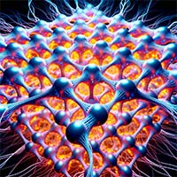
The crystal lattice defines the periodic arrangement of atoms
in a crystalline material. Lattice symmetry, atomic spacing, bonding, and
structural distortions can strongly influence the electronic band structure,
magnetism, phonons, and other collective excitations.
Electronic Band Structure
Atomic arrangement and crystal symmetry influence the allowed electronic
energy states in a solid. Changes in lattice structure can therefore alter
whether a material behaves as a metal, semiconductor, insulator, or
superconductor under particular conditions.
Symmetry & Topology
Crystal symmetries can protect or forbid certain electronic states and
band crossings. In topological materials, combinations of symmetry,
spin-orbit coupling, and electronic band structure can produce unusual
surface or edge states.
Electron Correlations
Lattice geometry and orbital overlap affect how strongly electrons interact.
In strongly correlated materials, these interactions can produce phenomena
that are difficult to explain using independent-electron models.
Electron-Phonon Interaction
Vibrations of the crystal lattice are described in terms of
phonons. Interactions between electrons and phonons can influence
electrical resistance, optical response, thermal transport, and some forms
of superconductivity.
Strain Engineering
Mechanical strain changes interatomic distances and crystal symmetry.
Researchers can therefore use substrate-induced strain, pressure, or
heterostructure design to modify electronic and magnetic properties and
explore new phases of matter.
How Are Quantum Materials Characterized?
Researchers combine structural, electronic, optical, magnetic, and transport
measurements to understand quantum-material behavior.
X-ray diffraction (XRD)
is commonly used to determine crystal structure, orientation, and phase.
Electron microscopy can provide atomic-scale structural information,
while neutron and X-ray scattering techniques can probe magnetic,
structural, and collective excitations.
Scanning tunneling microscopy (STM)
can measure surface electronic structure with atomic-scale spatial resolution.
Raman, FTIR, optical spectroscopy, ARPES, Hall measurements, resistivity
measurements, and magnetometry provide complementary information about
electronic, optical, vibrational, and magnetic behavior.
Quantum Materials Research Applications
Quantum-material research contributes to fields including
quantum information science, superconducting electronics,
spintronics, photonics, optoelectronics, advanced sensing, and
low-dimensional electronics.
Much of the field remains fundamental research. Researchers investigate
how crystal symmetry, electronic interactions, interfaces, dimensionality,
strain, temperature, magnetic fields, and external excitation can produce
or control new physical states.
Request Substrates for Quantum Materials Research
UniversityWafer supplies substrate options for experimental quantum-material
research, including single-crystal quartz, sapphire,
SiO2/Si, silicon, and other crystalline and dielectric materials.
When requesting a quote, specify the desired
material, diameter or dimensions, thickness, crystal orientation,
polish, surface roughness, coating or oxide thickness, optical requirements,
and quantity.
Related Quantum Materials & Research Substrates
Explore substrate materials, characterization methods, and fabrication topics commonly used in
quantum materials, condensed-matter physics, photonics, and thin-film research.
-
Single-Crystal Quartz Substrates
– Crystalline quartz for optical, dielectric, spectroscopy, and thin-film research applications.
-
Sapphire Wafers
– Electrically insulating crystalline substrates for optical, electronic, and quantum-material experiments.
-
SiO2/Si Wafers
– Oxide-coated silicon substrates for 2D materials, thin films, device fabrication, and transport measurements.
-
Graphene Research
– Explore graphene substrates and materials used in low-dimensional and quantum electronic research.
-
Materials Science Engineering
– Substrate materials and applications for advanced materials characterization and device development.
-
X-Ray Diffraction (XRD)
– Structural characterization of crystal phases, orientation, lattice parameters, and thin films.
-
Scanning Tunneling Microscopy (STM)
– Atomic-scale surface and electronic characterization of conductive quantum materials.
-
Graphene Under AFM Observations
– AFM characterization of graphene thickness, morphology, step edges, and substrate interactions.
-
Thin-Film Deposition
– Learn about deposition methods used to fabricate functional and quantum-material thin films.
