
Semiconductor Spectroscopy for Material Characterization
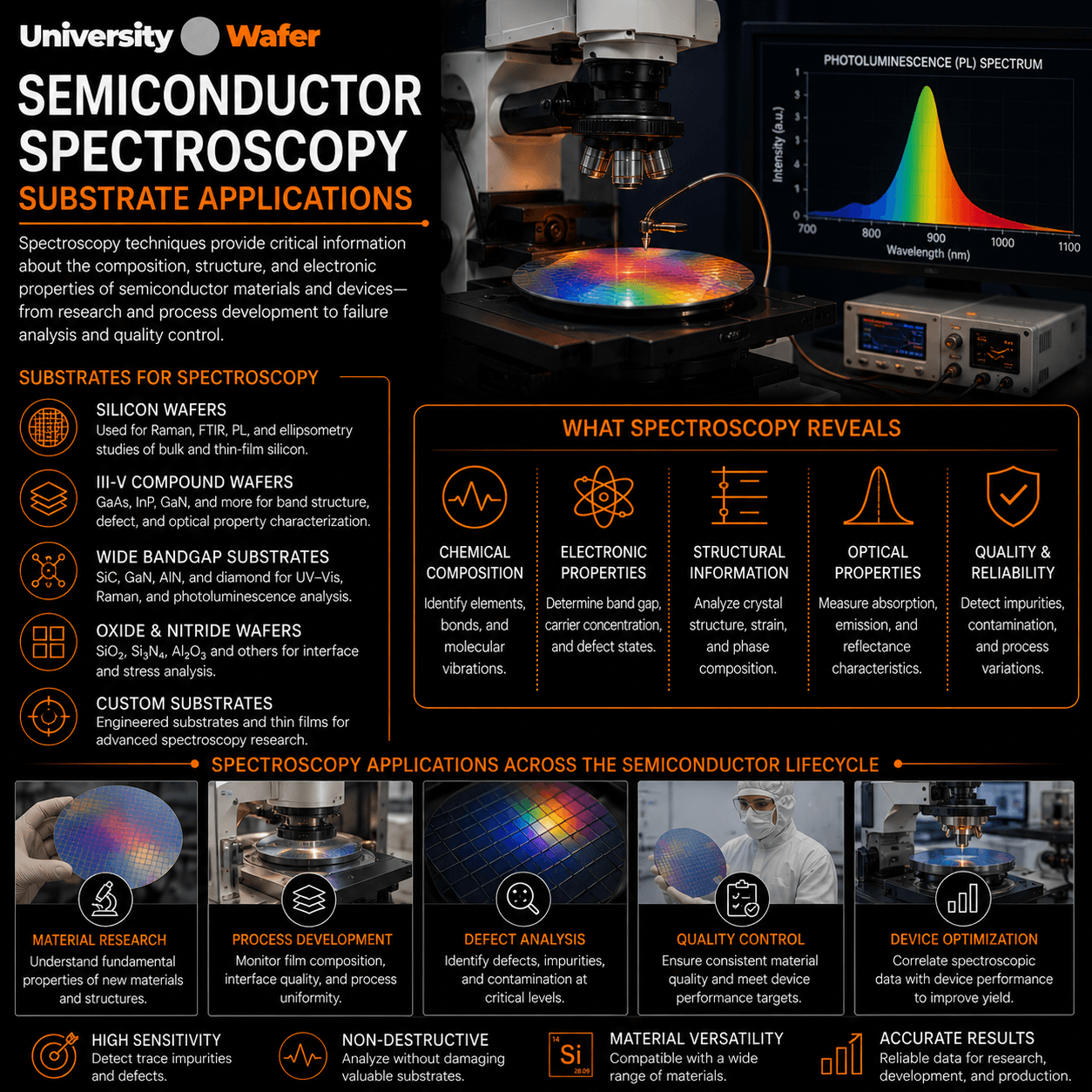
Semiconductor spectroscopy helps researchers investigate the optical, electrical, and structural properties of semiconductor materials without damaging the sample. Spectroscopic techniques are widely used to evaluate silicon wafers, compound semiconductors, epitaxial layers, quantum structures, and thin films throughout device development and manufacturing.
These analytical methods allow scientists to measure bandgap energy, carrier concentration, impurities, crystal defects, interface quality, and electronic transitions. The information obtained is essential for improving the performance of transistors, LEDs, lasers, solar cells, photodetectors, and other advanced semiconductor devices.
UniversityWafer supplies prime-grade silicon wafers, SOI wafers, GaAs, GaN, InP, and other research substrates for spectroscopy, photonics, and semiconductor characterization.
Get Your Semiconductor Wafer Quote FAST! Or, Buy Online and Start Researching Today!
Optical Coherence in Semiconductors
Optical coherence describes the phase relationship between photons and electronic states within a semiconductor. Understanding coherent interactions helps researchers investigate excitons, quantum wells, carrier dynamics, and light-matter interactions that influence laser performance, quantum devices, and ultrafast photonics.
Optical Excitation and Electronic Transitions
Optical excitation occurs when photons promote electrons between energy bands, allowing researchers to study band structure, excitonic effects, recombination processes, and defect states. These measurements provide valuable information for developing high-performance optoelectronic devices, including LEDs, laser diodes, photodetectors, and photovoltaic cells.
What Is Semiconductor Spectroscopy?
Semiconductor spectroscopy uses light, electrical signals, magnetic fields, or capacitance measurements to study the properties of semiconductor materials. These methods help researchers analyze silicon wafers, compound semiconductors, thin films, heterostructures, defects, interfaces, dopants, and optical behavior.
Spectroscopy is especially important in microelectronics, photonics, photovoltaics, MEMS, nanotechnology, and advanced device research because it can reveal how a material absorbs, emits, stores, or responds to energy.
Infrared Spectroscopy for Semiconductor Materials
Infrared spectroscopy measures how a semiconductor absorbs infrared light at different wavelengths. It is commonly used to study chemical bonding, impurities, hydrogen content, oxide layers, thin films, buried interfaces, and surface contamination.
For semiconductor processing, infrared methods such as FTIR can help characterize silicon dioxide films, wet chemical cleaning effects, and thin-film layers deposited on silicon or transparent substrates.
Capacitance Spectroscopy
Capacitance spectroscopy measures changes in capacitance to evaluate semiconductor interfaces, junctions, dopants, traps, and electronic defect states. It is often used with diodes, MOS structures, heterostructures, and semiconductor devices where charge storage and carrier behavior are important.
This technique can help identify interface trap density, depletion behavior, carrier concentration, and energy levels associated with defects. Researchers may use it to study semiconductor devices, solar cells, transistors, and dielectric layers.
Magnetic Resonance Spectroscopy
Magnetic resonance spectroscopy, including NMR and related techniques, uses magnetic fields to investigate the structure, composition, and chemical environment of semiconductor materials. It can provide information about bonding, impurities, dopants, and degradation products in thin films and device layers.
In semiconductor research, magnetic resonance methods may be used alongside optical and electrical spectroscopy to better understand material quality, defect chemistry, and electronic behavior.
Photoluminescence Spectroscopy
Photoluminescence spectroscopy is a non-destructive optical technique that measures light emitted by a semiconductor after it absorbs photons. It is widely used to evaluate bandgap energy, crystal quality, recombination mechanisms, impurities, defects, and strain in semiconductor wafers and epitaxial films.
Photoluminescence is especially useful for compound semiconductor materials such as GaAs, GaN, InP, and other optoelectronic materials used in LEDs, lasers, photodetectors, and solar cells.
Substrates Used for Spectroscopy Research
The choice of wafer substrate can affect spectroscopy results. Researchers often select wafers based on crystal orientation, resistivity, dopant type, surface roughness, oxide thickness, transparency, and contamination level.
- Silicon wafers for semiconductor spectroscopy and device characterization
- Thermal oxide wafers for oxide, dielectric, and interface studies
- SOI wafers for device and thin-film analysis
- GaAs wafers for photoluminescence and optoelectronic research
- GaN on sapphire wafers for LED, laser, and wide-bandgap semiconductor studies
- Fused silica wafers for optical and transmission measurements
Video: What is Semiconductor Spectroscopy?